
Page 31 - NEW Armstrong Book - 2
P. 31
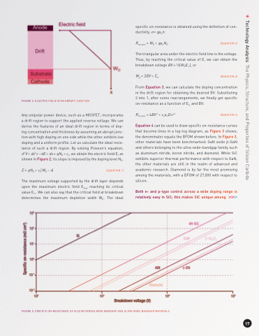
                                   FIGURE 2: ELECTRIC FIELD IN AN ABRUPT JUNCTION
Any unipolar power device, such as a MOSFET, incorporates a drift region to support the applied reverse voltage. We can derive the features of an ideal drift region in terms of dop- ing concentration and thickness by assuming an abrupt junc- tion with high doping on one side while the other exhibits low doping and a uniform profile. Let us calculate the ideal resis- tance of such a drift region. By solving Poisson’s equation, d 2V ÷ dx2 = –dE ÷ dx = qND ÷ εs, we obtain the electric field E, as shown in Figure 2; its slope is imposed by the doping level ND.
E = qND ÷ εs(WD – x) (EQUATION 1)
The maximum voltage supported by the drift layer depends upon the maximum electric field Emax reaching its critical value Ecr. We can also say that the critical field at breakdown determines the maximum depletion width WD. The ideal
specific on-resistance is obtained using the definition of con- ductivity, σ= qμnn:
Ron,spec = WD ÷ qμnND (EQUATION 2)
The triangular area under the electric field line is the voltage. Thus, by reaching the critical value of E, we can obtain the breakdown voltage BV = 1⁄2(WDEcr), or
WD = 2BV ÷ Ecr (EQUATION 3)
From Equation 3, we can calculate the doping concentration in the drift region for obtaining the desired BV. Substituting 2 into 1, after some rearrangements, we finally get specific on-resistance as a function of Ecr and BV:
Ron,spec = 4BV 2 ÷ εsμnEcr 3 (EQUATION 4)
Equation 4 can be used to draw specific on-resistance curves that become lines in a log-log diagram, as Figure 3 shows; the denominator equals the BFOM shown before. In Figure 3, other materials have been benchmarked: GaN oxide β-GaN and others belonging to the ultra-wide–bandgap family such as aluminum nitride, boron nitride, and diamond. While SiC exhibits superior thermal performance with respect to GaN, the other materials are still in the realm of advanced and academic research. Diamond is by far the most promising among the materials, with a BFOM of 27,000 with respect to silicon.
Both n- and p-type control across a wide doping range is relatively easy in SiC; this makes SiC unique among
    FIGURE 3: SPECIFIC ON-RESISTANCE OF SILICON VERSUS WIDE-BANDGAP AND ULTRA-WIDE–BANDGAP MATERIALS
 17
Technology Analysis The Physics, Structure, and Properties of Silicon Carbide
