
Page 186 - PCMI Journal December 2020
P. 186
PCM Educational Session for Colleges and New Staff
Presented by: David M. Allen, Emeritus Professor of Microengineering, Cranfield University, UK
11/23/20
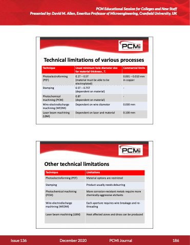
Technique
Usual minimum hole diameter size for material thickness , T.
Commercial limits
Photoelectroforming 0.1T – 0.5T
(PEF) (material must be able to be
0.001 – 0.010 mm in copper
-
Minimum aperture size
electroplated)
Stamping 0.5T – 0.75T
(dependent on material)
Photochemical machining (PCM)
0.8T
(dependent on material)
-
Wire-electrodischarge machining (WEDM)
Dependent on wire diameter
0.030 mm
Laser beam machining (LBM)
Dependent on laser and material
0.100 mm
45
46
Technical limitations of various processes
Other technical limitations
Technique
Limitations
Photoelectroforming (PEF)
Material options are restricted
Stamping
Product usually needs deburring
Photochemical machining (PCM)
More corrosion-resistant metals require more chemically-aggressive etchants
Wire-electrodischarge machining (WEDM)
Each aperture requires wire breakage and re- threading
Laser beam machining (LBM)
Heat affected zones and dross can be produced
Issue 136 December 2020 PCMI Journal 186
