
Page 278 - AWSAR 2.0
P. 278
254 || AWSAR Awarded Popular Science Stories - 2019
deposition, are needed and these require expensive vacuum chambers and deposition setups. Being a ceramic, ITO is brittle and has
stabilitycomparedtocopper.Inmywork,one- dimensional high aspect ratio nanostructures of silver (or in short, nanowires) were deposited on a substrate to form the TC. The wires had
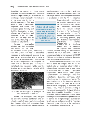
low areal density, which helped to maintain transparency and at the same time they formed an electrically conductive layer. The nanowire network is shown in Fig. 1, along with a spider web in the inset. To further improve the properties, a conducting polymer, poly (3, 4-ethylenedioxythiophene) polystyrene sulfonate (PEDOT:PSS in short),was mixed with the nanowires to improve their substrate
adhesion, without altering the optoelectronic properties. To ensure ease of fabrication, the nanocomposite (silver nanowires and PEDOT: PSS) was synthesized as a printable dispersion (ink), using a mixture of solvents.
Formulation of the nanocomposite as an ink has some advantages. The ink can be loaded onto any materials printer (inkjet or extrusion) and deposited over a wide range of substrates such as glass, polyethylene terephthalate (PET) sheets, photo paper, Kapton, to name a few. Printing is a widely used cost-effective deposition technique, which helps in conserving expensive material. The second advantage is that it enables selective deposition without the need for additional steps such as lithography or fabricated hard masks. Thus, inkjet or extrusion printing is highly advantageous at the design and testing stage, since it enables deposition of a variety of designs during product optimization. Once the design is fixed, commercial production can be carried out using techniques such as roll- to-roll, gravure, and screen printing. This might also entail some tailoring of the rheological properties of the nanocomposite ink.
poor toughness (breaks easily). formyworkwastofinda suitable substitute for ITO, with equal or better optoelectronic properties, but which also possesses good flexibility and ductility. Developing a cost- effective way of synthesis and deposition is also important, since this will help both in ease of manufacturing and in widespread adaptability.
The motivation
. Android authority statistics show nearly two screens are broken every second in the United States and the amount spend for replacement was more than $3.4 billion just in the year of 2018
Various engineering
solutions have their inspiration
from nature. For this work,
the inspiration is the spider, particularly its web. The spider’s web has two specialties: it appears to be transparent, because its low areal density structure has a lot of gaps, at the same time; the threads and their spacing are so cleverly optimized that the spider can catch even the smallest prey. This inspired me to fabricate a nanoscale “spider web” like structure using a conducting material, which will in effect act as a TC.
Fig. 1. Silver nanowire network on a substrate that resembles a spider’s web (inset)
Metals such as copper, silver, and gold are excellent electrical conductors and are collectively called noble metals. Among these, silver has the highest bulk conductivity, lower cost compared to gold, and greater corrosion
