
Page 106 - AWSAR_1.0
P. 106
AWSAR Awarded Popular Science Stories
the wastage of hardware resources. The modelling of the working of CSC solar cells showed that under ideal conditions, these cells have the potential to reach efficiency higher than the reported efficiencies till now in silicon solar cells.
The literature helped us to understand that the practical realization of CSC solar cells with TMO layers over silicon result in highly non-ideal surfaceand, hence, poor performance. In order to overcome the issue of the non-ideal surface of silicon and TMO, we incorporated a passivation layer using amorphous silicon (a-Si) to achieve better surface quality. We went ahead to understand the surface quality using a-Si by practically depositing the TMO layers and incorporating a-Si layer in between silicon and TMO surface. When we did the minority carrier lifetime measurement to understand the quality of the surface, we found that surface quality had improved more than 30 times by inserting the a-Si layer. This verified that we are on the right path and increased our curiosity level even more to see these solar cells working in real life.
But still, the satisfaction level was missing because there were still absorption losses in the thin layers that were obstructing the conversion of optical energy to electrical energy and, hence, hampering the performance of CSC solar cell. To eliminate these absorption losses, we came up with the idea to use these thin layers at the rear of the solar cells. This type of solar cell is proposed to absorb most of the light and convert it into electrical energy. Since this was a novel idea, we termed this type of design as Carrier Selective Back Contact (CSBC) solar cells. Modelling of CSBC solar cells showed that they can achieve efficiency close to maximum achievable efficiency in silicon solar cells.
The promising results for CSC and CSBC solar cells boosted our confidence and we went ahead to understand the physics underlying the working of CSC and CSBC solar cells. Best way to explain the working of these solar cells is through the development of mathematical equations. Hence, we first developed mathematical equations for these solar cells andthen decided the parameters to be obtained practically.
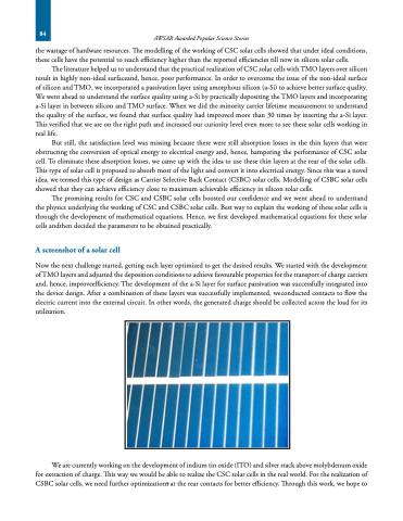
A screenshot of a solar cell
Now the next challenge started, getting each layer optimized to get the desired results. We started with the development of TMO layers and adjusted the deposition conditions to achieve favourable properties for the transport of charge carriers and, hence, improveefficiency. The development of the a-Si layer for surface passivation was successfully integrated into the device design. After a combination of these layers was successfully implemented, weconducted contacts to flow the electric current into the external circuit. In other words, the generated charge should be collected across the load for its utilization.
We are currently working on the development of indium tin oxide (ITO) and silver stack above molybdenum oxide for extraction of charge. This way we would be able to realize the CSC solar cells in the real world. For the realization of CSBC solar cells, we need further optimizations at the rear contacts for better efficiency. Through this work, we hope to
84
