Page 16 - RTH3BA Preview
P. 16
31 - �� ������������ � ��������� 2

            Suppose that both audio frequencies AF and carrier are applied with the
            instantaneous values as shown in Figure 31-2. The carrier input level is 6 to 8 times
            higher than the AF and, as such, determines which diodes will conduct. The arrows
            show the current produced by the carrier. With the polarities as shown, the audio
            voltage is assisting current flow through the top half of L5 and opposing current flow
            through the bottom half. The current through L5 is now upset (unbalanced) and an
            output at the sideband frequencies will appear in L6.

            In practice, some type of balancing of the circuit is required. This is usually a simple
            resistive voltage divider network, the resistance of which is adjusted to balance the
            modulator with the carrier only. In an SSB transmitter, this control is inside the
            transmitter on the circuit board and labelled carrier balance on the schematic
            diagram.

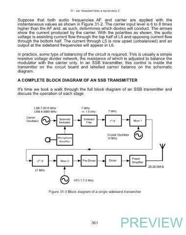
            A COMPLETE BLOCK DIAGRAM OF AN SSB TRANSMITTER


            It's time we took a walk through the full block diagram of an SSB transmitter and
            discuss the operation of each stage.


                               Figure 31-3 Block diagram of a single sideband transmitter


                                                                           PREVIEW
                                                          361

