
Page 105 - NEW Armstrong Book - 2
P. 105
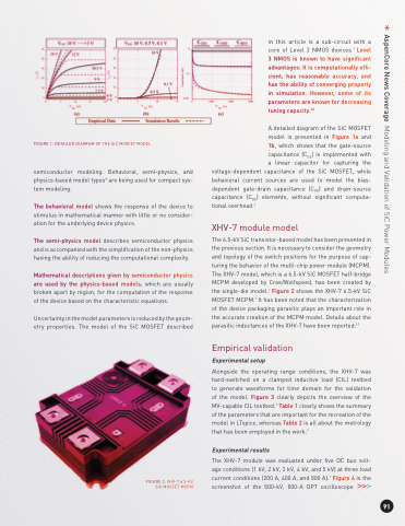
                                   FIGURE 1: DETAILED DIAGRAM OF THE SiC MOSFET MODEL
semiconductor modeling. Behavioral, semi-physics, and physics-based model types9 are being used for compact sys- tem modeling.
The behavioral model shows the response of the device to stimulus in mathematical manner with little or no consider- ation for the underlying device physics.
The semi-physics model describes semiconductor physics and is accompanied with the simplification of the non-physics having the ability of reducing the computational complexity.
Mathematical descriptions given by semiconductor physics are used by the physics-based models, which are usually broken apart by region, for the computation of the response of the device based on the characteristic equations.
Uncertainty in the model parameters is reduced by the geom- etry properties. The model of the SiC MOSFET described
in this article is a sub-circuit with a core of Level 3 NMOS devices.1 Level 3 NMOS is known to have significant advantages: It is computationally effi- cient, has reasonable accuracy, and has the ability of converging properly in simulation. However, some of its parameters are known for decreasing tuning capacity.10
A detailed diagram of the SiC MOSFET model is presented in Figure 1a and 1b, which shows that the gate-source capacitance (CGS) is implemented with a linear capacitor for capturing the
voltage-dependent capacitance of the SiC MOSFET, while behavioral current sources are used to model the bias- dependent gate-drain capacitance (CGD) and drain-source capacitance (CDS) elements, without significant computa- tional overhead.1
XHV-7 module model
The 6.5-kV SiC transistor-based model has been presented in the previous section. It is necessary to consider the geometry and topology of the switch positions for the purpose of cap- turing the behavior of the multi-chip power module (MCPM). The XHV-7 model, which is a 6.5-kV SiC MOSFET half-bridge MCPM developed by Cree/Wolfspeed, has been created by the single-die model.1 Figure 2 shows the XHV-7 6.5-kV SiC MOSFET MCPM.1 It has been noted that the characterization of the device packaging parasitic plays an important role in the accurate creation of the MCPM model. Details about the parasitic inductances of the XHV-7 have been reported.11
Empirical validation
Experimental setup
Alongside the operating range conditions, the XHV-7 was hard-switched on a clamped inductive load (CIL) testbed to generate waveforms for time domain for the validation of the model. Figure 3 clearly depicts the overview of the MV-capable CIL testbed.1 Table 1 clearly shows the summary of the parameters that are important for the recreation of the model in LTspice, whereas Table 2 is all about the metrology that has been employed in the work.1
Experimental results
The XHV-7 module was evaluated under five DC bus volt- age conditions (1 kV, 2 kV, 3 kV, 4 kV, and 5 kV) at three load current conditions (200 A, 400 A, and 800 A).1 Figure 4 is the screenshot of the 500-kV, 800-A DPT oscilloscope
 FIGURE 2: XHV-7 6.5-KV SiC MOSFET MCPM
    91
AspenCore News Coverage Modeling and Validation of SiC Power Modules
