
Page 120 - NEW Armstrong Book - 2
P. 120
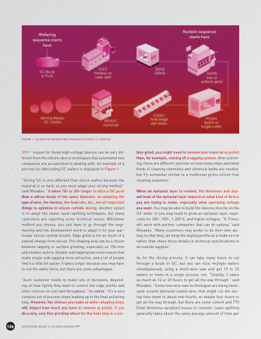
                                  FIGURE 1: SiC WAFER-PROCESSING SEQUENCE (SOURCE: X-TRINSIC)
niques for these high-voltage devices can be very dif- ferent from the silicon-device techniques that automated test companies are accustomed to dealing with. An example of a process for fabricating SiC wafers is displayed in Figure 1.
“Slicing SiC is very different than silicon wafers because the material is so hard, so you must adapt your slicing method,” said Rhoades. “It takes 10× or 20× longer to slice a SiC puck than a silicon boule of the same diameter, so adapting the type of wire, the tension, the feed rate, etc., are all important things to optimize in silicon carbide slicing. Another option is to adopt the newer laser-splitting techniques, but many customers are reporting some technical issues. Whichever method you choose, you just have to go through the engi- neering and the development work to adapt it for your par- ticular silicon carbide boules. Edge grind is not as much of a radical change from silicon. The shaping step can be a choice between lapping or surface grinding, especially on 150-mm and smaller wafers. Double-side lapping has some issues that make single-side lapping more attractive, and a lot of people find it a little bit easier. It takes longer because you may have to run the wafer twice, but there are some advantages.
“Each customer needs to make lots of decisions, depend- ing on how tightly they want to control the edge profile and other choices on cost and throughput,” he added. “It’s a very complex set of process steps leading up to the final polishing step. However, the choices you make at wafer-shaping steps will impact how much you have to remove at polish. If you do a very, very fine grinding wheel for the final step in a sur-
face grind, you might need to remove less material at polish than, for example, coming off a lapping system. After polish- ing, there are different opinions on how many steps and what kinds of cleaning chemistry and chemical baths are needed, but it’s somewhat similar to a traditional prime silicon final cleaning sequence.”
When an epitaxial layer is needed, the thickness and dop- ant level of the epitaxial layer depend on what kind of device you are trying to make, especially what operating voltage you want. You may be able to build the devices directly on the SiC wafer or you may need to grow an epitaxial layer, espe- cially for 600-, 900-, 1,200-V, and higher voltages. “X-Trinsic will work with partner companies that can do epitaxy,” said Rhoades. “Many customers may prefer to do their own epi- taxy so that they can keep the doping profile as a trade secret rather than share those details in technical specifications to an outside supplier.”
As for the slicing process, it can take many hours to cut through a boule of SiC, but you can slice multiple wafers simultaneously using a multi-wire saw and get 10 to 20 wafers or more in a single process run. “Usually, it takes as much as 16 or 20 hours to get all the way through,” said Rhoades. “Some new wire-saw technologies are being devel- oped around diamond-coated wire; that might cut the slic- ing time down to about one-fourth, so maybe four hours to get all the way through, but there are some control and TTV [total thickness variation] issues to consider. Laser splitting generally takes about the same average amount of time per
    106
ASPENCORE GUIDE TO SILICON CARBIDE
