
Page 73 - NEW Armstrong Book - 2
P. 73
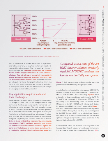
                                   FIGURE 2: COMPARISON OF THE TWO MOST COMMON TOPOLOGIES FOR 1,500-V PV INVERTERS
Ease of installation is another key feature of high-power, solar string inverters, as only two workers are needed to carry and install the system. Size and weight are therefore especially important. The latest generation of SiC semicon- ductors enables a significant increase in power-conversion efficiency. This not only saves energy but also results in smaller and lighter equipment with lower associated capi- tal, installation, and maintenance costs. Additional use cases are anticipated for home-charging infrastructure, often being linked to solar power generation and storage as well, albeit at lower power levels. At the end of this section, an example of a charging solution will be presented.
Key application requirements and
their challenges
Rising numbers of solar power modules with high-output DC voltages — up to 1,500 V — are being installed in large commercial facilities, as energy can be transferred more efficiently at higher voltages. The high operation voltage of 1,500 V in utility-scale installations requires optimized power semiconductor solutions. The special mission pro- files in these applications, combined with storage function- ality, mandate low cosmic-radiation–induced failure rates, along with a higher system efficiency for the power devices. Owing to these contradictory requirements, active neutral point clamped (ANPC) multilevel topologies have become the preferred solution because they enable the highest effi- ciency over the full range of power-factor operation, which is required for meeting bidirectional operation needs (see
Compared with a state-of-the-art IGBT inverter solution, similarly sized SiC MOSFET modules can handle substantially more power.
Figure 2). Such inverters are a perfect choice for both solar power conversion and battery storage applications.
A cost-effective way to exploit the advantages of SiC MOSFETs in ANPC topology is to combine Infineon’s 1,200-V CoolSiC MOSFET with TrenchStop IGBT7 technology. Figure 3 shows a phase leg of the proposed implementation, whereby T1, T4, T5, and T6 are composed of silicon-based IGBTs with cor- responding silicon freewheeling diodes. Transistors M2 and M3 consist of CoolSiC MOSFETs with internal body diodes. By using the modulation scheme1,2 presented in Figure 2, the IGBTs are switched continuously on or off with a grid fre- quency of 50/60 Hz only. Thus, switching losses are negligible for the IGBT. Therefore, IGBTs can be selected from the port- folio with a focus on low-conduction losses and the use of an optimized voltage rating. Switching losses occur only in the fast and highly efficient SiC MOSFETs.
Compared with IGBTs, SiC MOSFETs show very low turn-off losses and significantly reduced turn-on losses. Furthermore, they are nearly temperature-independent. By com-
    59
Technology Analysis What Makes SiC MOSFETs the Perfect Solution for String Inverters and Energy Storage Solutions?
