
Page 90 - NEW Armstrong Book - 2
P. 90
to the breakdown electric field. The on-resistance of the drift region is an important parameter. Analyzing the previous example of a p-n junction diode, we can see that the on- resistance is inversely proportional to the breakdown electric field for a uni- polar component.
The thinner semiconductor layers involve a lower density of minority charge carriers, an important param- eter for defining the reverse-recovery current. In fact, with other charac- teristics being equal, a component with a larger die designed to support higher currents will have a larger charge that undergoes the transient between conduction and interdic- tion and, therefore, will have a larger reverse-recovery current. The abil- ity of a semiconductor to switch to high frequency is directly proportional to its saturation drift speed, and the drift speed of SiC and gallium nitride is twice that of silicon. As a result, the latter can safely operate at higher frequencies. Also, a higher satura- tion drift rate is equivalent to faster removal of charges; this results in a shorter recovery time and a lower reverse-recovery current.
A wider bandgap allows high operating temperatures without sacrificing electrical characteristics.
The possibility of operating at high tem- peratures and a wider bandgap also depends on the thermal conductivity of the material. There are several ways to evaluate thermal resistance: You can analyze the thermal resistance between junction and case or the ther- mal resistance between junction and environment, for example.
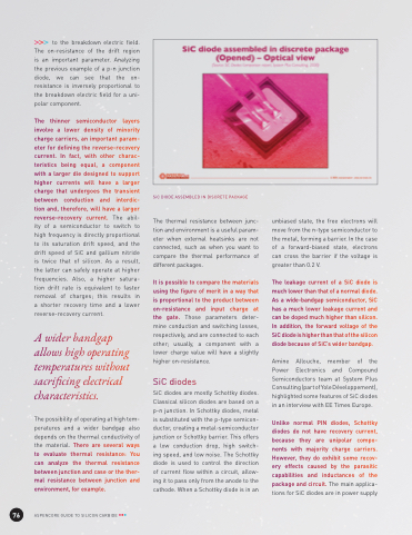
SiC DIODE ASSEMBLED IN DISCRETE PACKAGE
The thermal resistance between junc- tion and environment is a useful param- eter when external heatsinks are not connected, such as when you want to compare the thermal performance of different packages.
It is possible to compare the materials using the figure of merit in a way that is proportional to the product between on-resistance and input charge at the gate. Those parameters deter- mine conduction and switching losses, respectively, and are connected to each other; usually, a component with a lower charge value will have a slightly higher on-resistance.
SiC diodes
SiC diodes are mostly Schottky diodes. Classical silicon diodes are based on a p-n junction. In Schottky diodes, metal is substituted with the p-type semicon- ductor, creating a metal-semiconductor junction or Schottky barrier. This offers a low conduction drop, high switch- ing speed, and low noise. The Schottky diode is used to control the direction of current flow within a circuit, allow- ing it to pass only from the anode to the cathode. When a Schottky diode is in an
unbiased state, the free electrons will move from the n-type semiconductor to the metal, forming a barrier. In the case of a forward-biased state, electrons can cross the barrier if the voltage is greater than 0.2 V.
The leakage current of a SiC diode is much lower than that of a normal diode. As a wide-bandgap semiconductor, SiC has a much lower leakage current and can be doped much higher than silicon. In addition, the forward voltage of the SiC diode is higher than that of the silicon diode because of SiC’s wider bandgap.
Amine Allouche, member of the Power Electronics and Compound Semiconductors team at System Plus Consulting (part of Yole Développement), highlighted some features of SiC diodes in an interview with EE Times Europe.
Unlike normal PIN diodes, Schottky diodes do not have recovery current, because they are unipolar compo- nents with majority charge carriers. However, they do exhibit some recov- ery effects caused by the parasitic capabilities and inductances of the package and circuit. The main applica- tions for SiC diodes are in power supply
76
ASPENCORE GUIDE TO SILICON CARBIDE
