
Page 91 - NEW Armstrong Book - 2
P. 91
circuits but especially in power-factor– correction circuits in continuous con- duction mode, according to Allouche. SiC gives the diode a higher fault volt- age and higher current capacity, thus finding room in industrial charging.
“According to Yole Développement, the power SiC bare-die diode market was worth $160 million in 2019,” said Allouche. “This includes various market segments, such as automotive, energy, [and] industrial. ... In fact, SiC diodes are mainly used in medium-voltage applications [automotive, photovoltaics, motor control] to high-voltage applica- tions [smart power grid]. In automotive applications, SiC devices and particu- larly SiC diodes are currently adopted in on-board chargers.”
As with all SiC chips, the main chal- lenges faced by SiC diodes can be clas- sified into three levels, which Allouche detailed:
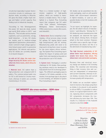
1. Material level. SiC wafers have a high production cost compared with Si wafers. The commercialized wafer size for SiC is still limited to 6 inches maxi- mum, whereas Si wafers are currently transitioning to 12 inches.
There is a limited number of high- volume suppliers of high-quality wafers, which are needed to manu- facture a reliable device. This is high- lighted in a System Plus Consulting report that compares raw SiC wafer costs from Infineon Technologies, Wolfspeed, Rohm Semiconductor, STMicroelectronics, onsemi, Microsemi, and UnitedSiC.
2. Device level. Device reliability is chal- lenging; critical process steps include SiC epitaxy, SiC doping (which needs high temperatures), and SiC etching. Manufacturing yields still need to be improved to bring them closer to yields for the more mature silicon technol- ogy. The System Plus Consulting report details the impact of epitaxy yield and wafer front-end manufacturing yield on the production cost of SiC diodes.
3. System level. Packaging is another challenge for SiC diodes. New packag- ing solutions need to be developed to fully benefit from SiC technology advan- tages. The different packaging aspects relevant to SiC diodes available on the market, from package type to die attach to wire bonding, are detailed in System Plus Consulting’s report.
SiC diodes can be assembled into dis- crete packaging, used as anti-parallel diodes with silicon-based transistors in hybrid modules, or used as anti- parallel diodes in full-SiC modules with SiC transistors.
“In our report, we highlight, for exam- ple, the die-attach choices of manufac- turers,” said Allouche. “Among the 11 SiC diodes by seven manufacturers that we analyzed, we observed five types of die attach. Among them, tin-based attach is the most common. However, one seller uses a specific type of high- performance die attach, but this is to the detriment of manufacturing costs.”
The high thermal conductivity of SiC allows better heat dissipation, offering smaller form factors than silicon. This allows lower costs and smaller packaging.
Recovery time and electrical recov- ery charge are shallow in SiC Schottky diodes. The essential and interesting thing is that recovery time and cur- rent are independent of temperature and current transients, whereas in sili- con diodes, recovery time and current increase greatly with temperature.
SiC diodes are an excellent replace- ment in inverters: By simply using them as diodes to be placed in anti-parallel to silicon IGBTs, it is possible to reduce losses. In a typical hybrid electric vehi- cle, replacing silicon components with SiC components increases the trac- tion efficiency by more than 10%. This results in a reduction of the heatsink volume to one-third.
This article was originally published on EE Times Europe on Dec. 3, 2020.
Maurizio Di Paolo Emilio is editor-in-chief of Power Electronics News and EEWeb.
SiC MOSFET DIE CROSS-SECTION
77
AspenCore News Coverage The Importance of SiC Semiconductors for Energy Efficiency
