


Page 1020 - Basic Electrical Engineering
P. 1020
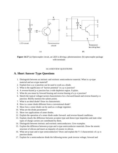
Figure 14.57 (a) Optocoupler circuit, an LED is driving a phototransistor; (b) optocoupler package
                                                        with terminals


                                                14.14 REVIEW QUESTIONS

               A. Short Answer Type Questions


                   1.  Distinguish between an intrinsic and extrinsic semiconductor material. What is a p-type
                     material and an n-type material?
                   2.  Explain how a p–n junction can be used to work as a diode.
                   3.  What is the significance of ‘barrier potential’ in a p–n junction?
                   4.  A reverse-biased p–n junction has a wide depletion region. Explain.
                   5.  What do you mean by forward biasing and reverse biasing of a p–n junction?
                   6.  Sketch the typical voltage/current characteristics for a forward-biased and reverse-biased p–n
                     junction. Briefly mention the salient points.
                   7.  What is an ideal diode? Draw its characteristic.
                   8.  How is a zener diode different from a conventional diode?
                   9.  Show how a zener diode can be used as a voltage regulator.
                 10.  What are the diode parameters?
                 11.  Show two applications of zener diodes.
                 12.  Explain the operation of a zener diode under forward- and reverse-biased conditions.
                 13.  Explain clearly the difference between acceptor-type and donor-type impurities and state what
                     types of charge carriers are contributed by them.
                 14.  Distinguish between intrinsic and extrinsic semiconductors. Give examples.
                 15.  Explain the difference between p-type and n-type semiconductor materials. Draw the atomic
                     structure of silicon and insert an impurity of arsenic in silicon.
                 16.  What are p-type and n-type semiconductors? Draw and explain the V–I characteristic of a p–n
                     junction diode.
                 17.  Explain for a semiconductor diode the following terms: peak inverse voltage; forward and

