
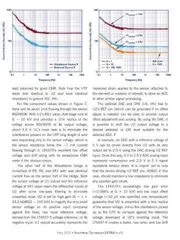
Page 16 - Industrial_Technology_EXTRA_May_11th_2020_Classical
P. 16
kept  balanced  for  good  CMR.  Note  how  the  UTP  measured strain applied to the sensor, attached to
       leads  look  identical  to  U2  and  have  identical  the element or material of interest, to drive an ADC
       impedance to ground (R2, R4).        or other similar signal processing.
         For  the  component  values  shown  in  Figure  2,  The  optional  DAC  and  OPA  (U4,  U5)  tied  to
       there will be about 1mA flowing through the sensor  U2’s REF pin (which can be grounded if no offset
       RSENSOR. With U1’s RG1 value, that stage runs at  adjust  is  needed)  can  be  used  to  provide  output
       G  =  10  V/V  and  provides  a  10×  replica  of  the  offset adjustment and zeroing. By using the DAC, it
       voltage  across  RSENSOR  at  its  output  voltage,  is  possible  to  shift  the  U2  output  voltage  to  a
       about  3.5  V.  U1’s  main  task  is  to  eliminate  the  desired  pedestal  or  CM  level  suitable  for  the
       interference present on the UTP long length of wire  selected ADC. F
       and responding only to the sensor voltage, which is  or example, an ADC with a reference voltage of
       the  sensor  resistance  times  the  ~1  mA  current  5  V  can  be  driven  directly  from  U2  with  its  zero
       flowing  through  it.  LT6370’s  excellent  low  offset  output set to 2.5 V using the DAC driving U2 REF
       voltage  and  drift  along  with  its  exceptional  CMR  input. Done this way, 0 V to 2.5 V ADC analog input
       make it the obvious choice.          represents  compression  and  2.5  V  to  5  V  signal
         The  other  half  of  the  Wheatstone  bridge  is  represents tension strain. It is import- ant to note
       comprised of R5, R6, and VR1 with near identical  that the device driving U2 REF pin, AD820 in this
       current flow as the sensor half of the bridge. Both  case, should maintain a low impedance to eliminate
       the sensor voltage at U1 output and the reference  any possible gain errors.
       voltage at VR1 wiper reach the differential inputs of  The  LT6370’s  exceedingly  low  gain  error
       U2  after  some  low-pass  filtering  to  eliminate  (<0.084%  at  G  =  10  V/V)  and  low  input  offset
       unwanted noise. U2 is set for high gain (G = 1 +  voltage (<50 µV max specified over temperature)
       24.2 kΩ/RG2 = 100 V/V) to magnify the very small  guarantee that U2 is presented with a true replica
       sensor  voltage  on  its  positive  input  compared  of the sensor voltage, minus the interference picked
       against  the  fixed,  low  noise  reference  voltage,  up  by  the  UTP,  to  compare  against  the  reference
       derived from the LT6657-5 voltage reference, on its  voltage  developed  at  U2’s  inverting  input.  The
       negative input. U1 output accurately represents the  LT6657-5 creates a stable, low noise, and low drift

                            May 2020 • INDUSTRIAL TECHNOLOGY EXTRA! • p16