Page 9 - ZS6KTS October 2019
P. 9
Circuit 2


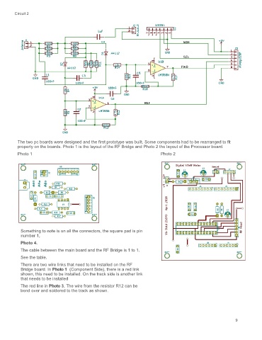
         The two pc boards were designed and the first prototype was built. Some components had to be rearranged to fit
         properly on the boards. Photo 1 is the layout of the RF Bridge and Photo 2 the layout of the Processor board.
         Photo 1                                                                                                            Photo 2


           Something to note is on all the connectors, the square pad is pin
           number 1,
           Photo 4.
           The cable between the main board and the RF Bridge is 1 to 1.
           See the table.
           There are two wire links that need to be installed on the RF
           Bridge board. In Photo 1  (Component Side), there is a red link
           shown, this need to be installed. On the track side is another link
           that needs to be installed
           The red line in Photo 3. The wire from the resistor R12 can be
           bend over and soldered to the track as shown.


                                                                                                                9

