
Page 3 - Carrier Recombination Activity and Structural Properties of Small-Angle Grain Boundaries in Multicrystalline Silicon
P. 3
Jpn. J. Appl. Phys., Vol. 46, No. 10A (2007) J. CHEN and T. SEKIGUCHI
Finally, to passivate the recombination activity of SA- allow diffusion followed by air cooling at a cooling rate of
GBs in mc-Si, hydrogen passivation was employed. The 30 K/s. According to the calculated solubility of Fe in Si, 25)
principle of H passivation is related to the annihilation of the approximate concentrations of Fe in the mc-Si samples
12
dangling bonds. 18,19) A former study has revealed that the annealed at 800, 900, 1000, and 1100 C were 3:0 10 ,
14
15
3
13
efficiency of H passivation on LA-GBs is affected by both 4:0 10 , 4:0 10 , and 3:0 10 cm , respectively.
the GB character and the impurity contamination level. 20) The Fe contamination level was categorized into three
However, because of the distinct structural difference groups, light (800 C), moderate (900–1000 C), and heavy
between LA- and SA-GBs, the passivation effect and (1100 C).
mechanism may be different. The effect of H passivation H passivation was conducted on as-grown mc-Si samples
on SA-GBs is discussed in §3.4. by H plasma treatment. Prior to H passivation, the mc-Si
In this study, the recombination activity of GBs is eval- samples were first observed using EBIC. The H plasma was
uated by temperature-dependent EBIC measurement. 21,22) generated at low pressure (16 Pa) with a radio frequency of
The GB character and misorientation angle are analyzed 13.56 MHz. The mc-Si samples were heated to 250 C for
by electron back-scattered diffraction (EBSD). 23) The GB 15 min. After H passivation, the mc-Si samples were once
structure was observed by transmission electron microscopy again prepared for a second EBIC observation.
(TEM). For the EBIC observation, samples were first mechan-
ically rubbed with carborundum followed by chemical
2. Experimental Procedure
polishing with CP4 solution. Schottky contacts were pre-
High purity mc-Si ingots were grown by controlled pared by depositing an Al layer (for p-type mc-Si) or Au
casting using the multi stage solidification control (MUST) layer (for n-type bonded Si) with a thickness of 25 nm on
method. 24) To reduce the residual impurity in the as-grown the sample surface. Ohmic contacts were prepared by Au
mc-Si ingot, semiconductor-grade Si was used as the raw deposition on the back surface. EBIC measurements were
material. In the MUST method, the solidification rate was performed using a TOPCON DS-130 scanning electron
changed step by step. At the first stage of crystal growth, the microscope (SEM) in the EBIC mode. 26) The acceleration
solidification rate was high at 0.5 mm/min, which enhances voltage was 20 kV and the beam current was 2.0 nA. EBIC
the initial crystal growth. Then, the solidification rate was contrast was defined by
reduced to 0.2 mm/min to suppress the generation of
C ¼ðI b I GB Þ=I b ; ð1Þ
defects. The size of the produced mc-Si ingot was 440
3
440 170 mm . The dopant was B with a concentration of where I b and I GB are the EBIC currents in the background
16
3
10 cm . The concentrations of O and C were in the order and at the GB, respectively. In addition to the EBIC
3
17
of 10 cm . Other impurities were analyzed by atomic measurement, EBSD analysis was carried out on the same
absorption spectrometry. The dominant metallic impurity samples to determine the GB character. EBSD observation
was Fe, the concentration of which was below 5 10 12 was performed using a LEO 1550 field-emission SEM in the
3
cm , at the center of the ingot. The Fe concentrations at the EBSD mode with an accelerating voltage of 25 kV. Finally,
bottom and top of the ingot were 1:6 10 15 and 1:3 10 16 some of the characterized samples were prepared for TEM
3
cm , respectively. Most of the other typical metal impu- observation at 200 kV.
rities were at concentrations lower than the detection limit,
14
3
except Al (less than 5 10 cm ). The average diffusion 3. Results and Discussion
length of minority carrier was about 250 mm, and the The GB characters in MUST mc-Si were analyzed from
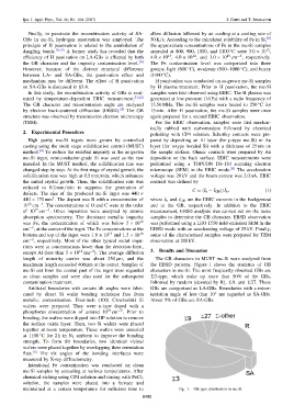
maximum length exceeded 400 mm at the center. Samples of the EBSD patterns. Figure 1 shows the statistics of GB
mc-Si cut from the central part of the ingot were regarded characters in mc-Si. The most frequently observed GBs are
as clean samples and were also used for the subsequent 3-type, which make up more than 50% of the GBs,
contamination treatment. followed by random (denoted by R), 9, and 27. These
Artificial boundaries with certain tilt angles were fabri- GBs are categorized as LA-GBs. Boundaries with a misor-
cated by direct Si wafer bonding technique free from ientation angle of less than 10 are regarded as SA-GBs.
metallic contamination. Four-inch (100) Czochralski Si About 5% of GBs are SA-GBs.
wafers were prepared. They were n-type doped with a
15
3
phosphorus concentration of around 10 cm . Prior to
bonding, the wafers were dipped into HF solution to remove
the surface oxide layer. Then, two Si wafers were placed
together at room temperature. These wafers were annealed
at 1100 C for 2 h in N 2 ambient to improve the bonding
strength. To form tilt boundaries, two identical vicinal
wafers were placed together by overlapping their orientation
flats. 16) The tilt angles of the bonding interfaces were
measured by X-ray diffractometry.
Intentional Fe contamination was conducted on clean
mc-Si samples by annealing at various temperatures. After
chemical etching using CP4 solution and rinsing with FeCl 3
solution, the samples were placed into a furnace and
maintained at a certain temperature for sufficient time to Fig. 1. GB-type distribution in mc-Si.
6490