
Page 17 - Electronics and Communication Engineering
P. 17
www.universityupdates.in || www.android.universityupdates.in || www.ios.universityupdates.in
Alpha developers and labs...
Alpha developers and labs...
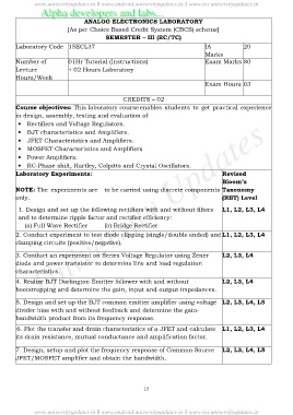
ANALOG ELECTRONICS LABORATORY
[As per Choice Based Credit System (CBCS) scheme]
SEMESTER – III (EC/TC)
Laboratory Code 15ECL37 IA 20
Marks
Number of 01Hr Tutorial (Instructions) Exam Marks 80
Lecture + 02 Hours Laboratory
Hours/Week
Exam Hours 03
CREDITS – 02
Course objectives: This laboratory course enables students to get practical experience
in design, assembly, testing and evaluation of
University Updates
· Rectifiers and Voltage Regulators.
· BJT characteristics and Amplifiers.
· JFET Characteristics and Amplifiers.
· MOSFET Characteristics and Amplifiers
· Power Amplifiers.
· RC-Phase shift, Hartley, Colpitts and Crystal Oscillators.
Laboratory Experiments: Revised
Bloom’s
NOTE: The experiments are to be carried using discrete components Taxonomy
only. (RBT) Level
1. Design and set up the following rectifiers with and without filters L1, L2, L3, L4
and to determine ripple factor and rectifier efficiency:
(a) Full Wave Rectifier (b) Bridge Rectifier
2. Conduct experiment to test diode clipping (single/double ended) and L1, L2, L3, L4
clamping circuits (positive/negative).
3. Conduct an experiment on Series Voltage Regulator using Zener L2, L3, L4
diode and power transistor to determine line and load regulation
characteristics.
4. Realize BJT Darlington Emitter follower with and without L2, L3, L4
bootstrapping and determine the gain, input and output impedances.
5. Design and set up the BJT common emitter amplifier using voltage L2, L3, L4, L5
divider bias with and without feedback and determine the gain-
bandwidth product from its frequency response.
6. Plot the transfer and drain characteristics of a JFET and calculate L1, L2, L3, L4
its drain resistance, mutual conductance and amplification factor.
7. Design, setup and plot the frequency response of Common Source L2, L3, L4, L5
JFET/MOSFET amplifier and obtain the bandwidth.
15
www.universityupdates.in || www.android.universityupdates.in || www.ios.universityupdates.in