
Page 378 - AWSAR 2.0
P. 378
354 || AWSAR Awarded Popular Science Stories - 2019
devices can be operated at ultra-high speeds! While the ultra-fast movement of charge across the junctions of 2D materials is well- known, we recently reported a lesser known mechanism of energy transfer at these junctions (see ACS nano 13.4 (2019): 4795- 4803). To understand this mechanism of energy transfer, let us gear up to dive little further into the monolayers of the flatland. In these monolayers, confinement of charges within a single sheet dramatically modifies the material properties. Attraction between the negative (electrons) and the positive (holes created by vacancy of electrons) charges, known as Coulomb interaction, increases as the charges are confined to the plane of monolayer. A simple analogy is to compare interaction between the people in a huge city versus a locked room. Because of strong Coulomb interaction in the monolayer, electron and hole start behaving as a single entity
called exciton.
An exciton can be thought
of as a hydrogen atom with
its own series of energy
states and the lowest of these
energy states now becomes
the primary bandgap of the semiconductor. One of the
ways of studying these exciton
states is by light exposure
where the light energy excites
carriers from valence band to
conduction band and forms
an exciton. As electron and
hole are strongly attracted to
each other, they recombine and emit light again, termed as photoluminescence (PL). Energy and intensity analysis of this PL spectrum helps to decode the exciton band structure and speculate various processes happening on light exposure. For example, if a heterojunction is made to separate electron and hole of an exciton formed in one of the
materials, PL intensity would decrease.
In our PL experiment, we designed a heterojunction from monolayer of Molybdenum Disulphide (MoS2) and multilayer Tin Diselenide (SnSe2). At the junction, energy alignment of SnSe2 states is at lower energies than the exciton states in MoS2. So, on light exposure, one would expect the population of excitons initially formed in MoS2 to be reduced as they move to lower energies in SnSe2 and, hence, anticipate a suppression of the PL intensity. On the contrary, we observe a dramatic increase in the MoS2 PL intensity by nearly ten times! This is possible because of an interesting matching inenergybetweentheexcitonstatesofMoS2 and certain energy states of SnSe2, where light absorption is the strongest. As an exciton is composed of electron and hole separated by some distance, it can act like an electric dipole, which is a simple form of antenna we come across in our daily lives. Because of energy resonance between MoS2 and SnSe2, dipoles in each material couple up and exchange energies similar to how a radio picks up the signal when it is tuned to the right channel. Such mechanism of energy transfer occurs in the nature during photosynthesis where sunlight absorbed by the chlorophyll molecule is transferred to the nearby reaction site for light harvesting. One of the reasons for observing energy transfer at the junction of 2D layers is the close spacing of two layers by just less than a nm where the dipoles can couple quite
strongly.
Usually, exciton dominated light
absorption in monolayers of 2D materials results in about utilization of ~10% of incident light, which is an exorbitant number that is unattainable with some materials even in the
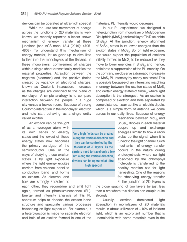
Very high fields can be created along the vertical direction and they can be controlled by the thickness of 2D layers. As the carriers need to travel only a few nm along the vertical direction, devices can be operated at ultra- high speeds!
