
Page 377 - AWSAR 2.0
P. 377
with its outside world through connection with a metal like copper and the device performance is critically controlled by this semiconductor- metal junction.
However, any defects at the interface between different materials in semiconductor heterojunctions disturbingly affects the device operation creating a bad surface for the charge flow. The surface of any material is very different from its bulk. The atoms at the surface are deprived of some of the bonds that the atoms in the bulk enjoy with the presence of neighbouring atoms in all the three directions. So, in a heterojunction, the interface is controlled by how the atoms on each material’s surface are satisfied by bonding with the atoms of the other. When the heterojunctions are grown in a semiconductor fab, growth of defect free interface needs a strenuous matching between the atomic spacings (lattice constants) of different materials, which otherwise leads to interface
strain. This puts a serious
limitation on the combination
of materials one can choose to
design a heterojunction.
To end this worry, voila, we
move into the fascinating world
of 2D materials the flatland.
Here in the flatland, materials
have atoms connected by
strong covalent bonds only
along the two directions while
in the third direction, atoms are
linked by rather weak bonds
known as van der Waal (vdW)
forces. You can imagine a 2D
material like a book where
several atomic sheets are just
held together by vdW forces. Using a simple apparatus consisting of a scotch tape and an optical microscope, these atomic sheets, or layers, can be peeled from a lump of material through a technique called micromechanical
Ms. Medha Dandu || 353
exfoliation. With some patience to endure the chaos of probability and training the eyes to adeptly identify the colour contrast of the exfoliated layers, we can obtain just a single sheet of 2D material called the monolayer, which is about less than a nanometer (nm) thick! Unlike in a 3D world, in the flatland, the surface of 2D materials does not crave for any bonds and, hence, can be integrated with any material as they can make a connection by means of vdW forces. Without worrying about the lattice mismatch, designing the heterojunctions in the flatland 2D layers is akin to playing with lego, that is, building blocks.
We, at the Quantum Electronics Laboratory (QEL) of Indian Institute of Science (IISc), are exploring hidden treasures of electronic and optical properties of heterojunctions in the flatland for useful device applications in light emission, harvesting and sensing. Heterojunctions made by vertically stacking
the 2D layers have many advantages and interesting properties. The junction is quite abrupt as you physically change the stacking material. While stacking the different 2D layers, their relative orientation can also be controlled which modifies properties according to the angle of stacking. When the interaction between two different monolayers can be tuned to be strong enough, they may no longer behave as two individual materials but start to have a different band structure altogether. Such junctions can be used to design artificial
semiconductors with required properties. Very high fields can be created along the vertical direction and they can be controlled by the thickness of 2D layers. As the carriers need to travel only a few nm along the vertical direction,
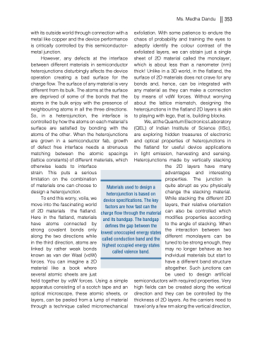
Materials used to design a
heterojunction is based on device specifications. The key factors are how fast can the charge flow through the material and its bandgap. The bandgap defines the gap between the lowest unoccupied energy states called conduction band and the highest occupied energy states called valence band.
