
Page 111 - NEW Armstrong Book - 2
P. 111
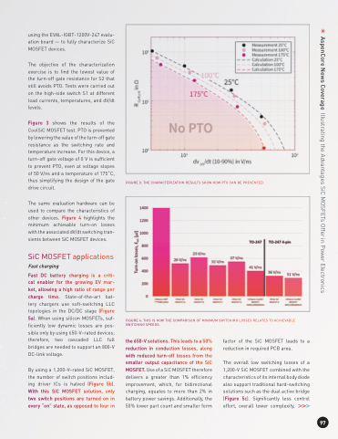
                                   using the EVAL-IGBT-1200V-247 evalu- ation board — to fully characterize SiC MOSFET devices.
The objective of the characterization exercise is to find the lowest value of the turn-off gate resistance for S2 that still avoids PTO. Tests were carried out on the high-side switch S1 at different load currents, temperatures, and dV/dt levels.
Figure 3 shows the results of the CoolSiC MOSFET test. PTO is prevented by lowering the value of the turn-off gate resistance as the switching rate and temperature increase. For this device, a turn-off gate voltage of 0 V is sufficient to prevent PTO, even at voltage slopes of 50 V/ns and a temperature of 175˚C, thus simplifying the design of the gate drive circuit.
The same evaluation hardware can be used to compare the characteristics of other devices. Figure 4 highlights the minimum achievable turn-on losses with the associated dV/dt switching tran- sients between SiC MOSFET devices.
SiC MOSFET applications
Fast charging
Fast DC battery charging is a criti- cal enabler for the growing EV mar- ket, allowing a high ratio of range per charge time. State-of-the-art bat- tery chargers use soft-switching LLC topologies in the DC/DC stage (Figure 5a). When using silicon MOSFETs, suf- ficiently low dynamic losses are pos- sible only by using 650-V–rated devices; therefore, two cascaded LLC full bridges are needed to support an 800-V DC-link voltage.
By using a 1,200-V–rated SiC MOSFET, the number of switch positions includ- ing driver ICs is halved (Figure 5b). With this SiC MOSFET solution, only two switch positions are turned on in every “on” state, as opposed to four in
FIGURE 3: THE CHARACTERIZATION RESULTS SHOW HOW PTO CAN BE PREVENTED.
 FIGURE 4: THIS IS HOW THE COMPARISON OF MINIMUM SWITCHING LOSSES RELATES TO ACHIEVABLE SWITCHING SPEEDS.
the 650-V solutions. This leads to a 50% reduction in conduction losses, along with reduced turn-off losses from the smaller output capacitance of the SiC MOSFET. Use of a SiC MOSFET therefore delivers a greater than 1% efficiency improvement, which, for bidirectional charging, equates to more than 2% in battery power savings. Additionally, the 50% lower part count and smaller form
factor of the SiC MOSFET leads to a reduction in required PCB area.
The overall low switching losses of a 1,200-V SiC MOSFET combined with the characteristics of its internal body diode also support traditional hard-switching solutions such as the dual active bridge (Figure 5c). Significantly less control effort, overall lower complexity,
    97
AspenCore News Coverage Illustrating the Advantages SiC MOSFETs Offer in Power Electronics
