
Page 110 - NEW Armstrong Book - 2
P. 110
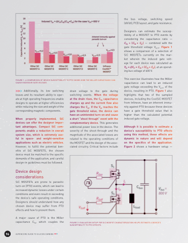
                                  FIGURE 1: A COMPARISON OF DEVICE SUSCEPTIBILITY TO PTO SHOWS HOW THE MILLER CAPACITANCE CAN CAUSE EXCESSIVE GATE VOLTAGE.
the bus voltage, switching speed (dV/dt), PCB layout, and gate resistance.
Designers can estimate the suscep- tibility of a MOSFET to PTO events by considering the capacitance ratio — Cdg ÷ (Cdg + Cgs) — combined with the gate threshold voltage Vgs,th. Figure 1 shows a comparison of a selection of SiC MOSFETs currently on the mar- ket wherein the induced gate volt- age for each device was calculated as Vgs = ΔVds × Cdg ÷ (Cdg + Cgs), at an operat- ing bus voltage of 600 V.
This exercise illustrates how the Miller capacitance can lead to an induced gate voltage exceeding the Vgs,th of the device, resulting in PTO. Figure 1 also highlights that two of the sampled devices, including the CoolSiC MOSFET from Infineon, have an inherent immu- nity against PTO because these devices have a gate threshold value that is higher than the calculated potential induced gate voltage.
Although it is possible to estimate a device’s susceptibility to PTO effects using this method, these effects are dynamic in nature and will depend on the specifics of the application. Figure 2 shows a hardware setup —
Additionally, its low switching losses and its resultant ability to oper- ate at high operating frequencies enable designs to operate at higher efficiencies while reducing the size and weight of the corresponding magnetic components.
When properly implemented, SiC devices can offer the designer impor- tant advantages. Compact SiC com- ponents enable a reduction in overall system size, which is extremely use- ful in space- and weight-sensitive applications such as electric vehicles. However, to fulfill the potential ben- efits of SiC MOSFETS, the chosen device must be matched to the specific demands of the application, and careful design-in guidelines must be followed.
Device design
considerations
SiC MOSFETs are prone to parasitic turn-on (PTO) events, which can lead to increased dynamic losses under certain conditions and even result in exceeding the device’s safe operating conditions. Designers should understand how any chosen device may suffer from PTO effects and how to prevent them.
A major cause of PTO is the Miller capacitance Cdg, which couples the
drain voltage to the gate during switching events. When the voltage at the drain rises, the Cdg capacitance charges up and the current flow also charges the Cgs. If the Vgs reaches the gate threshold value, the device can have an unintended turn-on and cause a short “shoot through” event with the complementary device. This generates additional power loss in the device. The severity of the shoot-through and the magnitude of the associated losses are related to the operating conditions of the MOSFET and the design of the asso- ciated circuitry. Critical factors include
    FIGURE 2: EVALUATION SETUP FOR SiC MOSFET CHARACTERIZATION HELPS ESTIMATE A DEVICE’S SUSCEPTIBILITY TO PTO EFFECTS.
 96
ASPENCORE GUIDE TO SILICON CARBIDE
