
Page 125 - NEW Armstrong Book - 2
P. 125
sistor (IGBT) in the late ’70s, which combined a MOSFET- like gate drive with a bipolar-like conduction path, giving the benefits of easy drive and a fixed saturation voltage so that power dissipation nominally increased proportionally to current rather than current squared, as in MOSFETs. IGBTs were not without their own problems, however, with a ten- dency to latch up, with catastrophic results. “Tail current” on switch-off also made dynamic losses relatively high, limiting operating frequency. The latch-up problem in modern IGBTs is now resolved and tail current minimized, while current and voltage ratings have increased dramatically, making the parts common in very high power conversion. Switching fre- quencies are still limited to a few tens of kilohertz maximum, though, because of dynamic losses.
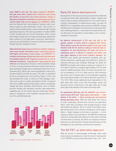
High switching frequencies are the key to smaller magnetics and overall smaller and lighter power-conversion products with higher-performance control loops, so as MOSFET on- resistance and voltage ratings have improved, they have been increasingly utilized, with frequencies pushed up to several hundreds of kilohertz, “superjunction” types being the state of the art. A limiting factor, however, is the breakdown voltage of silicon, forcing a minimum thickness of bulk material for a given operating voltage and a consequently high value of on- resistance (RDS). Many cells can be paralleled to reduce this, but then total die area (A) increases. The effect is quantified by the on-resistance per unit area (RDSA) figure of merit and has prompted the surge in interest in wide-bandgap mate- rials such as silicon carbide and gallium nitride. Compared with silicon, WBG materials have higher intrinsic breakdown voltage and other favorable characteristics, such as higher electron mobility and saturation velocity, high-temperature capability, and, for SiC, better thermal conductivity. Figure 1 shows a comparison of the headline characteristics of sili- con, SiC, and GaN materials.
Early SiC device developments
Development of SiC devices started a decade before GaN with an expected initial wider applicability to higher voltages and power rating. A natural starting point for a SiC switch was to consider development of enhancement-mode, normally off MOSFETs for compatibility with existing Si MOSFET designs and fabrication techniques. As with any new technology, there were teething problems — some that were predicted but oth- ers that were not and which caused delays to the commer- cialization of the parts.
An inherent characteristic of SiC was, and still is, the greater number of lattice defects compared with silicon. These defects cause low electron mobility at the gate-oxide interface with the SiC channel, leading to relatively high on- resistance. For cost effectiveness, SiC wafer size has to be maximized, and it is difficult to maintain low defect rate and wafer flatness at the 6-inch industry standard. SiC MOSFETs also exhibit gate-threshold instability with sig- nificant hysteresis, making gate drive difficult to design for optimum efficiency and reliability. Although the latest SiC MOSFETs are better and in theory could use a unipolar 0- to 15-V drive, in practice, a negative gate voltage of –5 V is often used for reliable operation. Also, 15 V does not give the low- est on-resistance, so 18 V is often used for best efficiency but at the cost of reduced short-circuit withstand capability and a decreased margin to the typical absolute maximum of 19 or 20 V. Other issues addressed were degradation of the gate oxide after short-circuit and overvoltage events and excessive electric field stress in the gate oxide due to high drain-gate field intensity in the device-blocking state.
An unpredicted difficulty with SiC MOSFETs was encoun- tered around 2010 with “basal plane dislocations” — bulk defects in the lattice — which actually grew and migrated during operating stress. With the body diode from source to drain conducting, electron-hole carriers are generated, which, when they recombine, have enough energy to move and enlarge the defects. This is a result of the higher band- gap energy value of SiC, and the consequence can be degra- dation — higher leakage current and on-resistance — in turn leading to higher losses and failure. SiC MOSFETs today have improved considerably with advances in fabrication methods and with defect screening, but efforts are ongoing to improve yield and cost-effectiveness of the die and performance of the packaging, for low inductance and thermal resistance.
The SiC FET: an alternative approach
With the arrival of wide-bandgap technology, while many semiconductor manufacturers took the route of development of SiC MOSFETs using existing fabrication lines, oth-
FIGURE 1: Si, SiC, AND GaN MATERIAL CHARACTERISTICS
111
Resources Origins of SiC FETs and Their Evolution Toward the Perfect Switch
