
Page 126 - NEW Armstrong Book - 2
P. 126
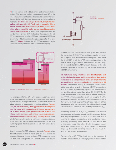
                                 ers started with a blank sheet and considered other options. The simplest switch implemented with SiC is the JFET structure, which has no gate oxide and is a unipolar con- duction device, so it does not show some of the limitations of MOSFETs. The device has a major drawback, though: It is nor- mally on with gate drive at 0 V and requires a negative drive to turn off. At best, this is inconvenient; at worst, it risks appli- cation failure, especially under transient conditions such as system turn-on/turn-off. A device was proposed in the ’90s and developed around 2010 that solved the problem: the SiC FET, a combination of a SiC JFET and a silicon MOSFET that is normally off but maintains the advantages of a JFET over a MOSFET. Figure 2 shows the SiC FET arrangement (right) compared with a generic SiC MOSFET schematic (left).
FIGURE 2: SiC MOSFET (LEFT) AND SiC FET CONSTRUCTION (RIGHT)
The arrangement of the SiC FET is a cascode, perhaps famil- iar to more mature engineers who may have even seen it implemented in its original form as a combination of vacuum tubes, intended to reduce noise in audio amplifiers. The cas- code, or “emitter switch,” has appeared in different guises over the years, with combinations of bipolar transistors or a BJT and a MOSFET; the general attribute is that a low- voltage switch controls a high-voltage one, with a good com- promise between high voltage rating and easy drive. Circuits with BJTs were not popular at high power, however, because of the significant base drive current necessary and the slow switching speed. The SiC cascode, or SiC FET, solves these problems.
Referring to the SiC FET schematic shown in Figure 3, when the Si MOSFET is turned on via its gate, the JFET source and gate are effectively shorted and the JFET conducts. Current can now pass through the JFET and MOSFET drain-source
FIGURE 3:
THE SiC FET SCHEMATIC
     112
ASPENCORE GUIDE TO SILICON CARBIDE
channels, with the conduction loss fixed by the JFET, because the low-voltage Si MOSFET on-resistance can be extremely low compared with that of the high-voltage SiC JFET. When the Si MOSFET is off, the JFET source voltage rises to the point at which its gate-source threshold of a few volts nega- tive is exceeded and the JFET turns off. Because of the ratio of device capacitances, dynamically, the voltage across the Si MOSFET remains low.
SiC FETs have many advantages over SiC MOSFETs, both in electrical performance and in practical use. As a switch, on-resistance is a major factor, and a SiC JFET inherently has much better electron mobility in the channel than a SiC MOSFET. The channel density is also higher and the combi- nation means that for a given die area, SiC FET on-resistance is 2× to 4× lower, or, conversely, up to 4× the number of dies can be obtained per wafer than with a SiC MOSFET for the same on-resistance. Compared with a silicon superjunc- tion MOSFET, the increased die count can be up to 13×. This increase in gross dies per wafer is critical to the success of the SiC FET technology, given that SiC as a material is likely always going to be more expensive than silicon. As discussed, a measure of the viability of a die is the figure of merit RDSA.
Another figure of merit is RDS × Eoss, or the tradeoff between on-resistance and device output switching energy, derived from output capacitance. This is a useful measure, as it is possible to reduce on-resistance and conduction losses by simply paralleling more cells in the die; but as well as increasing area, this also directly increases capaci- tance and consequently Eoss, which results in increased frequency-dependent switching losses. A low value for RDS × Eoss is therefore advantageous.
The gate of the SiC FET is simply that of the cascoded Si MOSFET. It has a stable, essentially hysteresis-free threshold
