
Page 127 - NEW Armstrong Book - 2
P. 127
of about 5 V and is therefore easy to drive with 12 V or 15 V for full enhancement and low RDS(on), with a large margin to the absolute maximum of typically 25 V. The easy SiC FET gate drive is nominally compatible with silicon MOSFET and even IGBT levels, giving potential backward-compatibility for exist- ing product design upgrades. SiC MOSFETs and certainly GaN HEMT cells in practice require custom drive arrangements for optimum efficiency and sufficient protection against over- voltage on the gates.
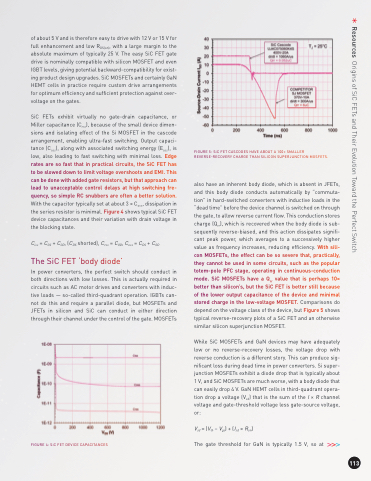
SiC FETs exhibit virtually no gate-drain capacitance, or Miller capacitance (Crss), because of the small device dimen- sions and isolating effect of the Si MOSFET in the cascode arrangement, enabling ultra-fast switching. Output capaci- tance (Coss), along with associated switching energy (Eoss), is low, also leading to fast switching with minimal loss. Edge rates are so fast that in practical circuits, the SiC FET has to be slowed down to limit voltage overshoots and EMI. This can be done with added gate resistors, but that approach can lead to unacceptable control delays at high switching fre- quency, so simple RC snubbers are often a better solution. With the capacitor typically set at about 3 × Coss, dissipation in the series resistor is minimal. Figure 4 shows typical SiC FET device capacitances and their variation with drain voltage in the blocking state.
Ciss = CGS + CGD, (CDS shorted), Crss = CGD, Coss = CDS + CGD
The SiC FET ‘body diode’
In power converters, the perfect switch should conduct in both directions with low losses. This is actually required in circuits such as AC motor drives and converters with induc- tive loads — so-called third-quadrant operation. IGBTs can- not do this and require a parallel diode, but MOSFETs and JFETs in silicon and SiC can conduct in either direction through their channel under the control of the gate. MOSFETs
FIGURE 4: SiC FET DEVICE CAPACITANCES
FIGURE 5: SiC FET CASCODES HAVE ABOUT A 100× SMALLER REVERSE-RECOVERY CHARGE THAN SILICON SUPERJUNCTION MOSFETS.
also have an inherent body diode, which is absent in JFETs, and this body diode conducts automatically by “commuta- tion” in hard-switched converters with inductive loads in the “dead time” before the device channel is switched on through the gate, to allow reverse current flow. This conduction stores charge (Qrr), which is recovered when the body diode is sub- sequently reverse-biased, and this action dissipates signifi- cant peak power, which averages to a successively higher value as frequency increases, reducing efficiency. With sili- con MOSFETs, the effect can be so severe that, practically, they cannot be used in some circuits, such as the popular totem-pole PFC stage, operating in continuous-conduction mode. SiC MOSFETs have a Qrr value that is perhaps 10× better than silicon’s, but the SiC FET is better still because of the lower output capacitance of the device and minimal stored charge in the low-voltage MOSFET. Comparisons do depend on the voltage class of the device, but Figure 5 shows typical reverse-recovery plots of a SiC FET and an otherwise similar silicon superjunction MOSFET.
While SiC MOSFETs and GaN devices may have adequately low or no reverse-recovery losses, the voltage drop with reverse conduction is a different story. This can produce sig- nificant loss during dead time in power converters. Si super- junction MOSFETs exhibit a diode drop that is typically about 1 V, and SiC MOSFETs are much worse, with a body diode that can easily drop 4 V. GaN HEMT cells in third-quadrant opera- tion drop a voltage (Vsd) that is the sum of the I × R channel voltage and gate-threshold voltage less gate-source voltage, or:
Vsd = (Vth – Vgs) + (Isd × Ron)
The gate threshold for GaN is typically 1.5 V, so at
113
Resources Origins of SiC FETs and Their Evolution Toward the Perfect Switch
