
Page 135 - NEW Armstrong Book - 2
P. 135
of merit (FOM) RDS × Eoss is therefore important when compar-
ing devices. Given similar R × E values, another differen- DS oss
tiating FOM is on-resistance per unit die area (R ). Small DS-A
values imply low device capacitances and higher yield from wafers for a given target on-resistance and consequent lower unit cost.
When comparing devices, the characteristics of the body diode or diode effect are important. In resonant converters, the inherent diode in a MOSFET conducts naturally during soft switching but is relatively poor-performance, with high forward-voltage drop and slow Qrr — which, at high frequency with short deadtimes, may be incomplete in the switching cycle, causing losses. WBG devices such as gallium nitride HEMT cells do not have a diode but conduct from source to drain in the “third quadrant” through the main channel rather than through the parasitic diode found in MOSFETs. Although there is no recovery charge in HEMT cells in third-quadrant conduction, the forward-voltage drop is also quite high, equal to the gate turn-on threshold voltage plus any negative “off” drive voltage applied. MOSFETs in WBG silicon carbide tech- nology have a parasitic diode; it’s fast, like a Schottky diode, but again, forward voltage is high, about 3 V. Although third- quadrant conduction time is short, losses can still be signifi- cant in the diode or diode effect when highest efficiency is needed. As a measure of the combination of channel conduc- tion and diode loss, RDS × Q is a useful FOM. SiC MOSFETs and GaN HEMT cells also have very sensitive gate drive require- ments for optimum efficiency.
SiC FETs’ advantages are being recognized in high-efficiency DC/DC converter applications using LLC and PSFB topologies.
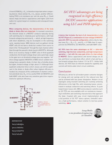
A device that includes the best of all characteristics is the SiC FET (Figure 6), a combination of a low-voltage Si MOSFET and a SiC JFET in a cascode configuration, which, like for like, has lower RDS-A, RDS × Eoss, and RDS × Q FOMs than Si super- junction (SJ) MOSFETs, SiC MOSFETs, and GaN HEMT cells.
SiC FETs have the same advantages as SiC — ultra-fast switching, high thermal conductivity, and high-temperature operation — but with the easy gate drive of a low-voltage Si MOSFET. Device capacitances and stored charge are all low, and there is a body diode effect, which is fast and has a low forward-voltage drop of about 1.5 V at 25˚C. Unlike GaN devices, SiC FETs have an inherent avalanche capability and current self-limits under short-circuit conditions.
Conclusion
Efficiency is a driver for all modern power-converter designs for energy and cost savings and for the reduced size that can be achieved with less power dissipation. Modern circuit topologies using resonant switching are routinely achieving efficiencies in the high 90s, with remaining losses concen- trated in residual conduction and switching effects. To push toward lower losses still, WBG semiconductor switches such as SiC FETs are now available with on-resistances measur- ing in milliohms and switching characteristics that approach the ideal. Coupled with easy circuit implementation and a full portfolio of SiC FET4 device options, UnitedSiC deliv- ers a high-performance, robust solution to low-loss power switching.
Anup Bhalla
is vice president of engineering at UnitedSiC.
FIGURE 6: THE SiC
FET — A CASCODE OF A Si MOSFET AND A SiC JFET
121
REFERENCES 1bit.ly/3AR0QFm 2prn.to/3zKnFtm 3bit.ly/3CHaVVX 4bit.ly/3u9ecKF
Resources New Semiconductor Technologies Are Driving Higher Efficiency in Power Conversion
