
Page 134 - NEW Armstrong Book - 2
P. 134
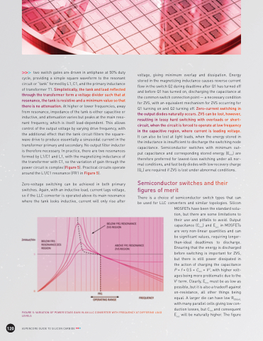
                                  two switch gates are driven in antiphase at 50% duty cycle, providing a simple square waveform to the resonant circuit or “tank” formed by L1, C1, and the primary inductance of transformer T1. Simplistically, the tank and load reflected through the transformer form a voltage divider such that at resonance, the tank is resistive and a minimum value so that there is no attenuation. At higher or lower frequencies, away from resonance, impedance of the tank is either capacitive or inductive, and attenuation varies but peaks at the main reso- nant frequency, which is itself load-dependent. This allows control of the output voltage by varying drive frequency, with the additional effect that the tank circuit filters the square- wave drive to produce essentially a sinusoidal current in the transformer primary and secondary. No output filter inductor is therefore necessary. In practice, there are two resonances formed by L1/C1 and L1, with the magnetizing inductance of the transformer with C1, so the variation of gain through the power circuit is complex (Figure 5). Practical circuits operate around the L1/C1 resonance (FR1 in Figure 5).
Zero-voltage switching can be achieved in both primary switches. Again, with an inductive load, current lags voltage, so if the LLC converter is operated above its main resonance where the tank looks inductive, current will only rise after
voltage, giving minimum overlap and dissipation. Energy stored in the magnetizing inductance causes reverse current flow in the switch Q2 during deadtime after Q1 has turned off and before Q1 has turned on, discharging the capacitance at the common switch connection point — a necessary condition for ZVS, with an equivalent mechanism for ZVS occurring for Q1 turning on and Q2 turning off. Zero-current switching in the output diodes naturally occurs. ZVS can be lost, however, resulting in lossy hard switching with overloads or short- circuit, when the circuit is forced to operate at low frequency in the capacitive region, where current is leading voltage. It can also be lost at light loads, when the energy stored in the inductance is insufficient to discharge the switching node capacitance. Semiconductor switches with minimum out- put capacitance and corresponding stored energy (Eoss) are therefore preferred for lowest-loss switching under all nor- mal conditions, and fast body diodes with low recovery charge (Qrr) are required if ZVS is lost under abnormal conditions.
Semiconductor switches and their
figures of merit
There is a choice of semiconductor switch types that can be used for LLC converters and similar topologies. Silicon MOSFETs have been the standard solu- tion, but there are some limitations to their use and pitfalls to avoid. Output capacitance (Coss) and Eoss in MOSFETs are very non-linear quantities and can be significant values, requiring longer- than-ideal deadtimes to discharge. Ensuring that the energy is discharged before switching is important for ZVS, but there is still power dissipated in the action of charging the capacitance P = f × 0.5 × Coss × V 2, with higher volt- ages being more problematic due to the V2 term. Clearly, Eoss must be as low as possible, but it is also a tradeoff against on-resistance, all other things being equal. A larger die can have low RDS(on), with many parallel cells giving low con- duction losses, but Coss and consequent Eoss will be naturally higher. The figure
    120
ASPENCORE GUIDE TO SILICON CARBIDE
FIGURE 5: VARIATION OF POWER STAGE GAIN IN AN LLC CONVERTER WITH FREQUENCY AT DIFFERING LOAD LEVELS
