
Page 142 - NEW Armstrong Book - 2
P. 142
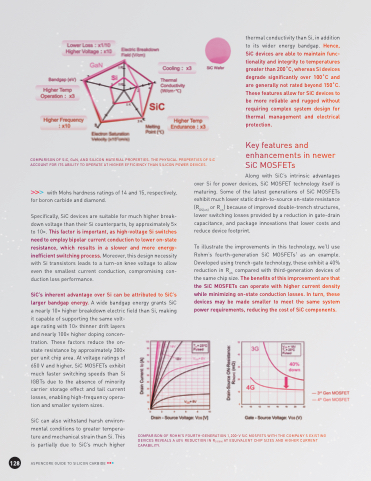
                                  COMPARISON OF SiC, GaN, AND SILICON MATERIAL PROPERTIES. THE PHYSICAL PROPERTIES OF SiC ACCOUNT FOR ITS ABILITY TO OPERATE AT HIGHER EFFICIENCY THAN SILICON POWER DEVICES.
thermal conductivity than Si, in addition to its wider energy bandgap. Hence, SiC devices are able to maintain func- tionality and integrity to temperatures greater than 200˚C, whereas Si devices degrade significantly over 100˚C and are generally not rated beyond 150˚C. These features allow for SiC devices to be more reliable and rugged without requiring complex system design for thermal management and electrical protection.
Key features and
enhancements in newer SiC MOSFETs
Along with SiC’s intrinsic advantages
with Mohs hardness ratings of 14 and 15, respectively, for boron carbide and diamond.
Specifically, SiC devices are suitable for much higher break- down voltage than their Si counterparts, by approximately 5× to 10×. This factor is important, as high-voltage Si switches need to employ bipolar current conduction to lower on-state resistance, which results in a slower and more energy- inefficient switching process. Moreover, this design necessity with Si transistors leads to a turn-on knee voltage to allow even the smallest current conduction, compromising con- duction loss performance.
SiC’s inherent advantage over Si can be attributed to SiC’s larger bandgap energy. A wide bandgap energy grants SiC a nearly 10× higher breakdown electric field than Si, making it capable of supporting the same volt-
age rating with 10× thinner drift layers and nearly 100× higher doping concen- tration. These factors reduce the on- state resistance by approximately 300× per unit chip area. At voltage ratings of 650 V and higher, SiC MOSFETs exhibit much faster switching speeds than Si IGBTs due to the absence of minority carrier storage effect and tail current losses, enabling high-frequency opera- tion and smaller system sizes.
SiC can also withstand harsh environ-
mental conditions to greater tempera-
ture and mechanical strain than Si. This
is partially due to SiC’s much higher CAPABILITY.
over Si for power devices, SiC MOSFET technology itself is maturing. Some of the latest generations of SiC MOSFETs exhibit much lower static drain-to-source on-state resistance (RDS(on) or Ron) because of improved double-trench structures, lower switching losses provided by a reduction in gate-drain capacitance, and package innovations that lower costs and reduce device footprint.
To illustrate the improvements in this technology, we’ll use Rohm’s fourth-generation SiC MOSFETs1 as an example. Developed using trench-gate technology, these exhibit a 40% reduction in Ron compared with third-generation devices of the same chip size. The benefits of this improvement are that the SiC MOSFETs can operate with higher current density while minimizing on-state conduction losses. In turn, these devices may be made smaller to meet the same system power requirements, reducing the cost of SiC components.
    128
ASPENCORE GUIDE TO SILICON CARBIDE
COMPARISON OF ROHM’S FOURTH-GENERATION 1,200-V SiC MOSFETS WITH THE COMPANY’S EXISTING DEVICES REVEALS A 40% REDUCTION IN RDS(ON) AT EQUIVALENT CHIP SIZES AND HIGHER CURRENT
