
Page 35 - NEW Armstrong Book - 2
P. 35
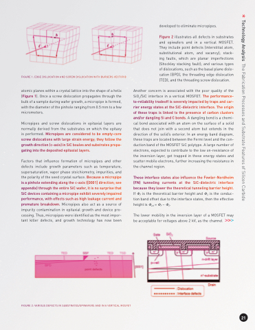
                                   FIGURE 1: EDGE DISLOCATION AND SCREW DISLOCATION WITH BURGERS VECTOR B
atomic planes within a crystal lattice into the shape of a helix (Figure 1). Once a screw dislocation propagates through the bulk of a sample during wafer growth, a micropipe is formed, with the diameter of the pinhole ranging from 0.5 mm to a few micrometers.
Micropipes and screw dislocations in epitaxial layers are normally derived from the substrates on which the epitaxy is performed. Micropipes are considered to be empty-core screw dislocations with large strain energy; they follow the growth direction (c-axis) in SiC boules and substrates propa- gating into the deposited epitaxial layers.
Factors that influence formation of micropipes and other defects include growth parameters such as temperature, supersaturation, vapor phase stoichiometry, impurities, and the polarity of the seed crystal surface. Because a micropipe is a pinhole extending along the c-axis ([0001] direction; see appendix) through the entire SiC wafer, it is no surprise that SiC devices containing a micropipe exhibit severely impaired performance, with effects such as high leakage current and premature breakdown. Micropipes also act as a source of impurity contamination in epitaxial growth and device pro- cessing. Thus, micropipes were identified as the most impor- tant killer defects, and growth technology has now been
Figure 2 illustrates all defects in substrates and epiwafers and in a vertical MOSFET. They include point defects (interstitial atom, substitutional atom, and vacancy); stack- ing faults, which are planar imperfections (Shockley stacking fault); and various types of dislocations, such as the basal plane dislo- cation (BPD), the threading edge dislocation (TED), and the threading screw dislocation.
Another concern is associated with the poor quality of the SiO2/SiC interface in a vertical MOSFET. The performance- to-reliability tradeoff is severely impacted by traps and car- rier energy states at the SiC-dielectric interface. The origin of these traps is linked to the presence of carbon clusters and/or dangling Si and C bonds. A dangling bond is a chemi- cal bond associated with an atom on the surface of a solid that does not join with a second atom but extends in the direction of the solid’s exterior. In an energy band diagram, these traps are located between the Fermi level and the con- duction band of the MOSFET SiC polytype. A large number of electrons, expected to contribute to the low on-resistance of the inversion layer, get trapped in these energy states and scatter mobile electrons, further increasing the resistance in the channel region.
These interface states also influence the Fowler-Nordheim (FN) tunneling currents at the SiC-dielectric interface because they lower the theoretical tunneling barrier height. If ΦF is the theoretical barrier height and ΦC is the conduc- tion band offset due to the interface states, then the effective height is Φeff = ΦF – ΦC.
The lower mobility in the inversion layer of a MOSFET may be acceptable for voltages above 2 kV, as the channel
developed to eliminate micropipes.
    FIGURE 2: VARIOUS DEFECTS IN SUBSTRATES/EPIWAFERS AND IN A VERTICAL MOSFET
 21
Technology Analysis The Fabrication Processes and Substrate Features of Silicon Carbide
