
Page 45 - NEW Armstrong Book - 2
P. 45
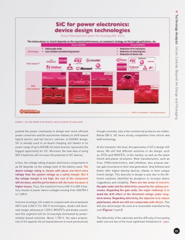
                                   FIGURE 1: SiC FOR POWER ELECTRONICS, DEVICE DESIGN TECHNOLOGIES
pushed the power community to design ever-more efficient power converters and the automotive industry to shift toward hybrid electric and full electric vehicles. In EV/HEV design, SiC is already used in on-board charging, but thanks to its power range of up to 400 kW, the main inverter represents the biggest opportunity for SiC. Moreover, the new idea of using 800-V batteries will increase the potential of SiC devices.
In fact, the voltage rating of power electronics components in an EV depends on the voltage level of the battery used. The device voltage rating is chosen with about one-third extra voltage than the system voltage as a safety margin. But if the voltage margin is too high, the cost of the component will increase, and the performance will decrease because of higher losses. Thus, the transition from a 400-V to 800-V bat- tery results in power device voltages moving from 650/700 V to 1,200 V.
In terms of voltage, SiC is able to compete with silicon between 600 V and 3,300 V. For 650-V technologies, diodes will domi- nate longer, whereas at 1,200 V, MOSFETs and diodes coexist, and this segment will be increasingly dominated by power- module–based solutions. Above 1,700 V, the value proposi- tion of SiC against silicon-based devices is more pronounced,
though currently, only a few commercial products are visible. Below 500 V, SiC faces strong competition from silicon and GaN technology.
At the transistor die level, the panorama of SiC’s design still varies. We still find different solutions to die design, such as JFETs and MOSFETs, in the market, as well as the latest trench and planar structures. Most manufacturers, such as Cree, STMicroelectronics, and Littelfuse, also propose pla- nar gate structures in their new generation. Only Infineon and Rohm offer higher-density devices, thanks to their unique trench design. This diversity in design is also due to the dif- ferent solutions identified by designers to increase device ruggedness and reliability. There are two areas of concern: the gate oxide and the defectivity caused by the epitaxy pro- cesses. Regarding the gate oxide, the major challenge is to avoid the drift effect of the threshold voltage under long- term stress. Regarding defectivity, the objective is to reduce yield losses, which are still not comparable with silicon. This will also allow larger die sizes at a reasonable manufacturing cost (Figures 1 and 2).
The defectivity of the substrate and the difficulty of increasing wafer size are two of the most significant limitations in
     31
Technology Analysis Silicon Carbide: Beyond the Design and Packaging
