
Page 46 - NEW Armstrong Book - 2
P. 46
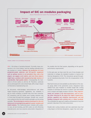
                                   FIGURE 2: IMPACT OF SiC ON MODULE PACKAGING
this phase of growing demand. Currently, mass pro- duction is on 4-inch wafers, and the leading manufacturers are moving to 6 inches. However, the production of 6-inch production-grade substrate and SiC-specific equipment such as epitaxy reactors is not prevalent; thus, only a few players can supply 6-inch wafers, and even those players might have a problem with manufacturing high volumes of reproducible, high-quality wafers. Consequently, the tran- sition to 8-inch wafers is still far off. Therefore, substrate prices and equipment costs remain high, with a major impact on final device manufacturing cost.
As discussed, wide-bandgap semiconductors will allow higher-frequency–operation capabilities, but reliability is key for these modules to benefit fully from their potential. SiC transistors and SiC diodes were initially released only in three-lead through-hole packages, though now, several more advanced discrete and module packages are becoming available. The technological solutions developed for discrete devices are increasingly being applied in power modules and small modules. The traditional power modules with a plas- tic case, all wire bonding, and SAC solder are still offered by manufacturers, but new solutions allow better integration of
the module into the final system, depending on the specific performance requirements.
In the past year, we have seen the use of new designs and materials to reshape the standard modules to improve the thermal dissipation of SiC. The innovations spread through- out all manufacturing levels, from the encapsulation to the heatsink.
New hard resins are now available as alternatives to the clas- sic epoxy, while in the automotive sector, integrators have shifted from case modules to molded single-side cooling modules to eliminate the need for a plastic case and enable more compact and highly modular inverters. Thus, improve- ments are needed in die interconnections, such as over- lay, silver sintering for die attach (for higher temperature- junction capability and reliability improvement), and ball bonding (compared with existing wire or ribbon bonding). The embedded die approach enables achievement of very low parasitic inductance from interconnections.
Double-side cooling modules and new substrates have had a big impact on thermal dissipation; copper has seen wide-
    32
ASPENCORE GUIDE TO SILICON CARBIDE
