
Page 57 - NEW Armstrong Book - 2
P. 57
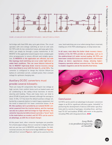
                                   FIGURE 4: EV AUXILIARY DC/DC CONVERTER TOPOLOGIES — DAB (LEFT) AND CLLC (RIGHT)
full bridge with fixed 50% duty cycle gate drives. The circuit operates with zero-voltage switching at turn-on and suits SiC FETs with its low conduction losses and easy gate drive, which can simply be through a pulse transformer. A SiC MOSFET in this application would require more complex gate drive arrangements to ensure efficient and reliable opera- tion. Si MOSFETs in the application are efficient, but with this topology, hard switching can occur under light-load or under-fault conditions. This can cause failures induced by the Si MOSFET high-body–diode reverse-recovery energy but is less likely to occur with the lower Qrr of SiC FETs. The converter is configured to charge the traction lithium-ion battery in controlled current, constant power, then constant voltage for optimum charging rate.
Auxiliary DC/DC converters must
provide several kilowatts
There are many EV components that require low voltage at high current, from comfort items such as heated seats and air conditioning to the safety-critical functions of electric steering and braking. These and many more can total to about 20 kW of peak power demand, although the average is lower. In EVs, 12 V has been the default auxiliary voltage rail, backed by a separate battery to match legacy equipment, but the trend is toward 48 V for lower connection losses. In an EV, this auxiliary rail is provided by an isolated DC/DC con- verter powered from the traction battery, and the topology can also be a phase-shift full bridge for high efficiency. The converter may also be bidirectional to provide a “boost” back to the main battery as needed, and SiC FETs can be used to an advantage, as with the on-board charger.
At this power level, other converter topologies are possible. For a fixed output voltage, the LLC converter is highly efficient and can use low-cost Si MOSFETs and fast diodes. For bidi- rectional versions, the dual active bridge (DAB) (see Figure 4, left) and CLLC version (Figure 4, right) can be used, but in this
case, hard switching can occur when energy flow is reversed, making use of SiC FETs advantageous, to keep losses low.
In all cases, even when the better diode recovery charac- teristics of the SiC FETs provide no advantage, such as in the unidirectional LLC under normal loading, SiC FETs can have lower conduction losses and switch faster, with smaller delays as device capacitances charge, allowing higher- frequency operation without excessive loss. This then leads to smaller magnetics and all the benefits that follow.
 Conclusion
SiC FETs can be used to an advantage in all power-conversion stages in an EV for significant efficiency gains. UnitedSiC3 is pioneering the development of devices with better specifica- tions and in a variety of packages, including three- and four- lead TO-247 and leadless DFN88, with more in the pipeline, including IPMs with integrated drivers.
Anup Bhalla
is vice president of engineering at UnitedSiC.
      43
Technology Analysis SiC Use Proliferates in New EV Designs
