
Page 81 - NEW Armstrong Book - 2
P. 81
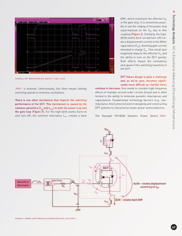
                                   FIGURE 4: DPT WAVEFORMS (SiC MOSFET, 1,200 V, 40 A)
is minimal. Unfortunately, this often means limiting switching speeds to minimize oscillations.
There is one other mechanism that impacts the switching performance of the DUT. This mechanism is caused by the common parasitics (Cgd and LPL2) in both the power loop and the gate loop (Figure 5). For the high-di/dt events (turn-on and turn-off), the common inductance LPL2 creates a back
EMF, which minimizes the effective VGS in the gate loop. It is sometimes possi- ble to see the ringing of the power loop superimposed on the VGS due to this coupling (Figure 2). Similarly, the high- dV/dt events (turn-on and turn-off) cre- ate a displacement current in the Miller capacitance (Cgd), diverting gate current intended to charge Cgs. This result also negatively impacts the effective VGS and the ability to turn on the DUT quickly. Both effects impact the consistency and speed of the switching transition of the DUT.
DPT fixture design is quite a challenge and, as we’ve seen, becomes signifi- cantly more difficult as rise/fall times
continue to decrease. One needs to consider high-frequency effects of multiple second-order circuits (loops) and is often limited in the ability to minimize parasitic inductances and capacitances. Fundamental technology barriers (e.g., low- inductance interconnects) exist in designing and constructing DPT systems to characterize newer power semiconductors.
The Keysight PD1500A Dynamic Power Device
       FIGURE 5: POWER LOOP PARASITICS MINIMIZING GATE LOOP DRIVE
 67
Technology Analysis SiC Is Essential to Advancing EV and Energy Infrastructure
