
Page 79 - NEW Armstrong Book - 2
P. 79
more than a 100% error.
Let’s run Scenario #2 again with a DPT fixture designed for a 200-MHz bandwidth and see how much impact that will have on the result.
Result: The displayed value on the oscilloscope has only a 2% error. This is a significant improvement in results by design- ing the fixture for a 200-MHz bandwidth.
Conclusion: Common instruments, like oscilloscopes, are more than capable of supporting the needs of a high-speed DPT system.
(Note: Because our analysis involves two poles, we must consider the relationship between rise time and band- width for second-order systems. Simple second-order cir- cuit simulation was performed to
approximate the ratio. The graphed result shows the tr × f3dB product to be close to 0.35 for (0.5 < ζ < 1.0); for (0.05 ζ < 0.5), the ratio drops to only ~0.27. Therefore, our conclusion remains valid for second-order sys- tems.2 A more significant challenge to providing repeatable and reliable results involves the design of the DPT fixture, including connection of the measurement probes.)
Considerations for DPT
fixture design
Cgd, Rg, Ls). Power semiconductor manufacturers continue to develop new packaging materials and designs to minimize the stray parasitics. But once you determine your power semiconductor of choice, the focus is on external parasitics within the fixture.
There are three loops that are worth considering when ana- lyzing the double-pulse waveforms (VGS, VDS, ID): the DC-link loop, the gate loop, and the power loop (Figure 3). As always, it is good practice to minimize the area of the loop, which is proportional to the total loop inductance. This can be done practically by routing PCB traces (main and return) close to each other, or by using twisting pairs if routing the signals through wires.
The DC-link loop should be considered when the DC-link capacitor charging the load inductor (L) is interrupted (i.e., when the DUT is turned off). When the DUT is turned off, the current charged up in L recirculates through the body diode in the high-side MOSFET. Therefore, there is no cur- rent coming from the DC-link capacitor, and the DC-link stray
Because of the faster rise/fall times
(i.e., higher bandwidths) required for
newer power semiconductors, analy-
ses of the fixture layout and circuit
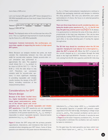
parasitics are critical to provide repeatable and reliable DPT waveforms. If the DPT waveforms are not repeatable and reliable, they often have second-order underdamped oscillations of the pulsed waveforms (VGS, VDS, ID), making it impossible to extract repeatable dynamic characterization parameters (e.g., e(on), e(off)) (Figure 2).
Figure 3 shows the DPT setup with the primary parasitic capacitances, inductances, and resistances that need to be considered when designing your DPT fixture. Some of these parasitics are inherent in the power devices themselves (e.g.,
FIGURE 2: TURN-OFF PULSES FROM A GaN DEVICE (VDS = 100 V, ID = 10 A, VGS = 12 V)
inductance (LDC-Link) has a large –di/dt. LDC-Link resonates with the decoupling capacitor in parallel with parasitic output capacitance from the half bridge, developing a voltage surge across VDC and VDS. This resonant oscillation can be seen on VDS in Figure 4 during both turn-off events. It can also be seen in Figure 2 as the lower-frequency oscillation of VDS. It is next to impossible to eliminate this oscillation, but care needs to be taken to minimize it.
For the gate loop, the main parasitics you have control over in your fixture layout are LGL and LPL2. It is often not
65
Technology Analysis SiC Is Essential to Advancing EV and Energy Infrastructure
