
Page 80 - NEW Armstrong Book - 2
P. 80
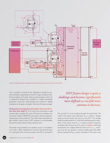
                                  FIGURE 3: PRIMARY PARASITICS NEEDING CONSIDERATION DURING DPT SWITCHING TRANSIENTS
possible to minimize this inductance enough to pre- vent oscillation, depending on the DUT’s gate resistance (Rg). If the oscillation still exists, then an external gate resistor Rg is required to dampen the oscillation to enable repeatable parameter extraction. Unfortunately, the tradeoff in adding resistance to the gate is a slower rise time of the gate voltage.
SiC geometries are typically much smaller than Si and there- fore often have larger Rg. So it may not be necessary to add external gate resistance to some SiC devices to dampen the oscillation, while Si MOSFETs may require external dampen- ing because of the smaller Rg. One often finds many different gate resistor values used in DPT systems to accommodate the specific power device being characterized.
The power loop parasitics are another source of oscillation in VDS and ID. After ramping the current to the desired value in L, during the first of the two pulses, the DUT is turned off.
DPT fixture design is quite a challenge and becomes significantly more difficult as rise/fall times continue to decrease.
The current in L is recirculated through the body diode. The –di/dt in the power loop inductance (LPL1) creates a voltage surge across the drain and source of the DUT. This voltage surge resonates with the Cds of the DUT and the parasitic induc- tance of the power loop (LPL1), creating a higher-frequency oscillation that can be seen in VDS and ID in Figure 2. Although mechanisms are slightly different from turn-on, LPL1 contin- ues to be the key parasitic involved. Additionally, with WBG devices having low RDS(on) values, damping of the power loop
    66
ASPENCORE GUIDE TO SILICON CARBIDE
