


Page 1027 - Basic Electrical Engineering
P. 1027
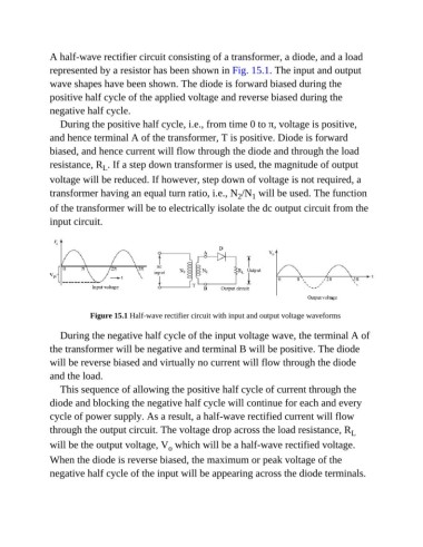
A half-wave rectifier circuit consisting of a transformer, a diode, and a load
               represented by a resistor has been shown in Fig. 15.1. The input and output
               wave shapes have been shown. The diode is forward biased during the

               positive half cycle of the applied voltage and reverse biased during the
               negative half cycle.

                  During the positive half cycle, i.e., from time 0 to π, voltage is positive,
               and hence terminal A of the transformer, T is positive. Diode is forward

               biased, and hence current will flow through the diode and through the load
               resistance, R . If a step down transformer is used, the magnitude of output
                               L
               voltage will be reduced. If however, step down of voltage is not required, a
               transformer having an equal turn ratio, i.e., N /N  will be used. The function
                                                                          1
                                                                      2
               of the transformer will be to electrically isolate the dc output circuit from the
               input circuit.


                           Figure 15.1 Half-wave rectifier circuit with input and output voltage waveforms

                  During the negative half cycle of the input voltage wave, the terminal A of
               the transformer will be negative and terminal B will be positive. The diode

               will be reverse biased and virtually no current will flow through the diode
               and the load.

                  This sequence of allowing the positive half cycle of current through the
               diode and blocking the negative half cycle will continue for each and every

               cycle of power supply. As a result, a half-wave rectified current will flow
               through the output circuit. The voltage drop across the load resistance, R              L

               will be the output voltage, V  which will be a half-wave rectified voltage.
                                                  o
               When the diode is reverse biased, the maximum or peak voltage of the

               negative half cycle of the input will be appearing across the diode terminals.

