
Page 14 - 8237A (1)
P. 14
8237A
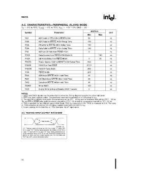
A.C. CHARACTERISTICSÐPERIPHERAL (SLAVE) MODE
T A e 0§Cto70§C, T CASE e 0§Cto75§C, V CC ea 5V g5%, GND e 0V
8237A-5
Symbol Parameter Unit
Min Max
TAR ADR Valid or CS LOW to READ LOW 50 ns
TAW ADR Valid to WRITE HIGH Setup Time 130 ns
TCW CS LOW to WRITE HIGH Setup Time 130 ns
TDW Data Valid to WRITE HIGH Setup Time 130 ns
TRA ADR or CS Hold from READ HIGH 0 ns
TRDE Data Access from READ LOW (Note 5) 140 ns
TRDF DB Float Delay from READ HIGH 0 70 ns
TRSTD Power Supply HIGH to RESET LOW Setup Time 500 ns
TRSTS RESET to First IOWR 2TCY ns
TRSTW RESET Pulse Width 300 ns
TRW READ Width 200 ns
TWA ADR from WRITE HIGH Hold Time 20 ns
TWC CS HIGH from WRITE HIGH Hold Time 20 ns
TWD Data from WRITE HIGH Hold Time 30 ns
TWWS Write Width 160 ns
TWR End of Write to End of Read in DMA Transfer 0 ns
NOTES:
1. DREQ and DACK signals may be active high or active low. Timing diagrams assume the active high mode.
2. EOP is an open collector output. This parameter assumes the presence of a 2.2K pullup to V CC .
3. The net IOW or MEMW Pulse width for normal write will be TCYb100 ns and for extended write will be 2TCYb100 ns.
The net IOR or MEMR pulse width for normal read will be 2TCYb50 ns and for compressed read will be TCYb50 ns.
4. TDQ is specified for two different output HIGH levels. TDQ1 is measured at 2.0V. TDQ2 is measured at 3.3V. The value
for TDQ2 assumes an external 3.3 KX pull-up resistor connected from HRQ to V CC .
5. Output Loading on the Data Bus is 1 TTL Gate plus 100 pF capacitance.
A.C. TESTING INPUT/OUTPUT WAVEFORM
231466–12
A.C. Testing: Inputs are driven at 2.4V for a Logic ‘‘1’’ and 0.45V
for a Logic ‘‘0.’’ Timing measurements are made at 2.0V for a
Logic ‘‘1’’ and 0.8V for a Logic ‘‘0.’’ Input timing parameters as-
sume transition times of 20 ns or less. Waveform measurement
points for both input and output signals are 2.0V for HIGH and
0.8V for LOW, unless otherwise noted.
14