
Page 12 - 8237A (1)
P. 12
8237A
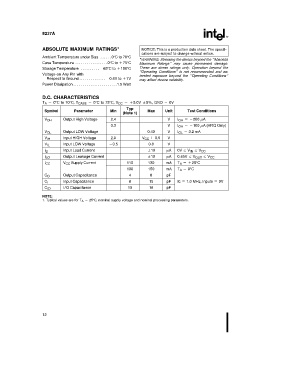
ABSOLUTE MAXIMUM RATINGS* NOTICE: This is a production data sheet. The specifi-
cations are subject to change without notice.
Ambient Temperature under Bias ÀÀÀÀÀÀ0§Cto70§C
*WARNING: Stressing the device beyond the ‘‘Absolute
Case Temperature ÀÀÀÀÀÀÀÀÀÀÀÀÀÀÀÀÀ0§Cto a 75§C Maximum Ratings’’ may cause permanent damage.
Storage Temperature ÀÀÀÀÀÀÀÀÀÀ b65§Cto a 150§C These are stress ratings only. Operation beyond the
‘‘Operating Conditions’’ is not recommended and ex-
Voltage on Any Pin with
tended exposure beyond the ‘‘Operating Conditions’’
Respect to GroundÀÀÀÀÀÀÀÀÀÀÀÀÀÀ b0.5V to a 7V may affect device reliability.
Power DissipationÀÀÀÀÀÀÀÀÀÀÀÀÀÀÀÀÀÀÀÀÀÀÀ1.5 Watt
D.C. CHARACTERISTICS
T A e 0§Cto70§C, T CASE e 0§Cto75§C, V CC ea 5.0V g5%, GND e 0V
Typ
Symbol Parameter Min Max Unit Test Conditions
(Note 1)
V OH Output High Voltage 2.4 V I OH eb200 mA
3.3 V I OH eb100 mA (HRQ Only)
V OL Output LOW Voltage 0.40 V I OL e 3.2 mA
V IH Input HIGH Voltage 2.0 V CC a 0.5 V
V IL Input LOW Voltage b0.5 0.8 V
I LI Input Load Current g10 mA 0V s V IN s V CC
I LO Output Leakage Current g10 mA 0.45V s V OUT s V CC
I CC V CC Supply Current 110 130 mA T A ea 25§C
130 150 mA T A e 0§C
C O Output Capacitance 4 8 pF
C I Input Capacitance 8 15 pF fc e 1.0 MHz, Inputs e 0V
C IO I/O Capacitance 10 18 pF
NOTE:
e 25§C, nominal supply voltage and nominal processing parameters.
1. Typical values are for T A
12