
Page 39 - NEW Armstrong Book - 2
P. 39
thin the substrate to reduce device resistance or facilitate processing of wafers with thick epitaxy. Metals CTE-matched to SiC, such as molybdenum, tungsten, and titanium- tungsten, are deposited for device reliability and ruggedness.
Foundry inspection tools that make use of optical metrology are now commercially available for SiC wafers, which are transparent to visible wavelengths. Substrate and epitaxy researchers are working vigorously to improve SiC material planarity. In addition, fabrication engineers are optimizing processes (such as high-temperature implantation anneal- ing) that can exacerbate the relative lack of SiC wafer planar- ity. Finally, deposited insulation dielectrics, which are prone to defect incorporation, are rigorously investigated with respect to their impact on edge-termination performance and device stability.
SiC etch
Etching SiC is crucial in trench MOSFET fabrication. Because of its hardness, SiC is not attacked by single acids at room temperature. Therefore, corrosive mixtures at high tem- peratures are required for wet etching. Disadvantages of this include the need for specialized and dedicated clean-room equipment and areas and the inability to perform preferential etches with conventional masking materials. As a result, dry- etching techniques such as reactive-ion etching (RIE) and ICP etching have been developed with practical etch rates and good selectivity for deep SiC patterning. Commercial RIE systems developed for Si can be used to etch SiC. Etching gas systems are typically fluorine-based, chlorine-based, or bromine-based:
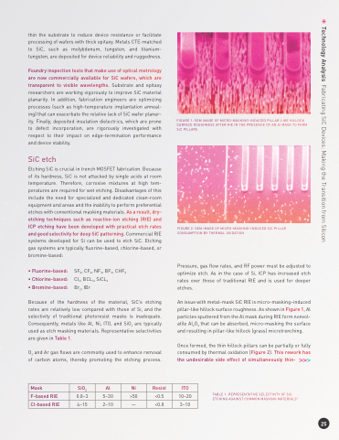
FIGURE 1: SEM IMAGE OF MICRO-MASKING–INDUCED PILLAR-LIKE HILLOCK SURFACE ROUGHNESS AFTER RIE IN THE PRESENCE OF AN Al MASK TO FORM SiC PILLARS
FIGURE 2: SEM IMAGE OF MICRO-MASKING–INDUCED SiC PILLAR CONSUMPTION BY THERMAL OXIDATION
Pressure, gas flow rates, and RF power must be adjusted to optimize etch. As in the case of Si, ICP has increased etch rates over those of traditional RIE and is used for deeper etches.
An issue with metal-mask SiC RIE is micro-masking–induced pillar-like hillock surface roughness. As shown in Figure 1, Al particles sputtered from the Al mask during RIE form nonvol- atile Al2O3 that can be absorbed, micro-masking the surface and resulting in pillar-like hillock (grass) microtrenching.
Once formed, the thin hillock pillars can be partially or fully consumed by thermal oxidation (Figure 2). This rework has the undesirable side effect of simultaneously thin-
TABLE 1: REPRESENTATIVE SELECTIVITY OF SiC ETCHING AGAINST COMMON MASKING MATERIALS2
• Fluorine-based: • Chlorine-based: • Bromine-based:
SF6, CF4, NF3, BF3, CHF3 Cl2, BCL3, SiCL4
Br2, IBr
Because of the hardness of the material, SiC’s etching rates are relatively low compared with those of Si, and the selectivity of traditional photoresist masks is inadequate. Consequently, metals like Al, Ni, ITO, and SiO2 are typically used as etch masking materials. Representative selectivities are given in Table 1.
O2 and Ar gas flows are commonly used to enhance removal of carbon atoms, thereby promoting the etching process.
Mask
SiO2
Al
Ni
Resist
ITO
F-based RIE
0.8–3
5–30
>50
<0.5
10–20
Cl-based RIE
4–15
2–10
—
<0.8
3–10
25
Technology Analysis Fabricating SiC Devices: Making the Transition from Silicon
