
Page 41 - NEW Armstrong Book - 2
P. 41
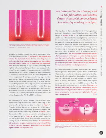
                                   FIGURE 5: SEM IMAGE OF WAFER SURFACE AFTER COMPLETION OF FURNACE HIGH-TEMPERATURE POST ION-IMPLANTATION THERMAL ANNEALING IN THE PRESENCE OF A PROTECTIVE CAP LAYER
As stated, irradiating SiC with ions during implantation dam- ages the crystal structure. To recrystallize the material and activate the implanted atoms, thermal annealing must be performed. For improved surface quality and morphology, post-implantation anneal can be done under gas flow condi- tions. Furnace annealing or rapid thermal annealing utiliz- ing high-intensity flash lamps or lasers can be used. In the case of furnace annealing, temperatures in excess of 1,300˚C are common. A concern with annealing at high temperatures or under high-vacuum conditions is surface degradation by silicon evaporation. By using a protective cap layer over the wafer surface during the annealing process, surface degra- dation can be minimized. Graphite, SiO2, Si3N4, AlN, BN/AlN, and carbon-protective annealing cap layers are commonly used. Carbon cap layers yield excellent results. They can be formed by RF sputtering or graphitization of photoresist. No chemical reactions occur at the SiC/carbon interface. At completion of annealing, the carbon cap can be removed by ashing (O2 plasma) or 700˚C to 800˚C oxidation.
An SEM image of a wafer surface that underwent post- implantation high-temperature furnace annealing in the absence of a protective cap layer is shown in Figure 4. Extensive surface damage has occurred. An SEM image of a SiC wafer that was capped with graphite during post ion- implantation thermal annealing is shown in Figure 5. With the exception of the absence of protective annealing capping on the wafer surface of Figure 4, the two wafers contained SiC JFETs of identical design and underwent identical pro- cessing as part of the same fabrication lot. At completion of fabrication, the uncapped wafer yielded no functional JFETs, in sharp contrast to the capped wafer, which had a relatively high functional device yield of 85%.
Ion implantation is exclusively used in SiC fabrication, and selective doping of material can be achieved by employing masking techniques.
The signature of the ion bombardment of the implantation process is visible in the dotted SiC surface texture in the SEM images of Figures 4 and 5. The high furnace temperature and the ease of removal of the capping layer at completion of thermal annealing are the primary considerations in choos- ing a suitable capping layer material. After completion of ion- implantation annealing, thermal and deposited dielectrics are utilized for surface passivation and reliability purposes. Combinations of thermal and high-temperature–densified deposited oxides as well as sacrificial oxidations are com- monly performed. The effectiveness of the surface passiv- ation is evidenced by low gate-to-source leakage currents and sharp onsets of voltage breakdowns that contribute to device reliability. Orders-of-magnitude reduction in SiC p-n junction leakage current can be achieved by use of optimized thermal and sacrificial oxidation passivation.
Ion implantation and subsequent high-temperature anneal- ing can generate defects that degrade device performance. These include complex point defects, localized levels (shal- low or deep), extended defects (basal plane dislocation loops and stacking faults), and new dislocations and/or move- ment of existing dislocations. These defects can degrade device performance and are a reliability concern. Thus, the ion-implantation process must be improved. The goal is to optimize annealing and the overall implantation process to minimize defect generation and to develop high-quality, room-temperature, heavy-dose ion implantation for low- cost manufacturing.
FIGURE 6: CROSS-SECTIONAL SEM IMAGE OF HEAVILY DOPED P+ IMPLANTED GATE REGIONS IN N-CHANNEL. THE IMPLANT STRAGGLE UNDERCUTTING THE MASK IS NOTED.
      27
Technology Analysis Fabricating SiC Devices: Making the Transition from Silicon
