
Page 42 - NEW Armstrong Book - 2
P. 42
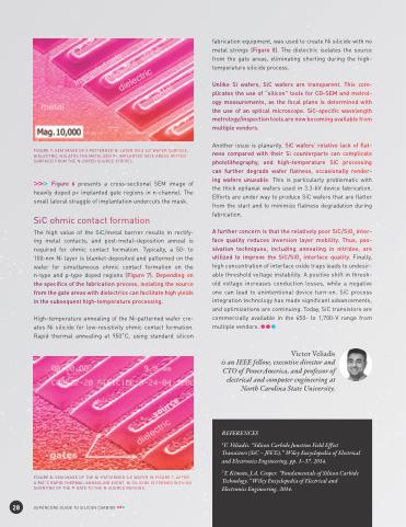
                                 FIGURE 7: SEM IMAGE OF A PATTERNED Ni LAYER ON A SiC WAFER SURFACE. DIELECTRIC ISOLATES THE METALIZED P+ IMPLANTED GATE AREAS (PITTED SURFACE) FROM THE N-DOPED SOURCE STRIPES.
Figure 6 presents a cross-sectional SEM image of heavily doped p+ implanted gate regions in n-channel. The small lateral straggle of implantation undercuts the mask.
SiC ohmic contact formation
The high value of the SiC/metal barrier results in rectify- ing metal contacts, and post-metal–deposition anneal is required for ohmic contact formation. Typically, a 50- to 100-nm Ni layer is blanket-deposited and patterned on the wafer for simultaneous ohmic contact formation on the n-type and p-type doped regions (Figure 7). Depending on the specifics of the fabrication process, isolating the source from the gate areas with dielectrics can facilitate high yields in the subsequent high-temperature processing.
High-temperature annealing of the Ni-patterned wafer cre- ates Ni silicide for low-resistivity ohmic contact formation. Rapid thermal annealing at 950˚C, using standard silicon
FIGURE 8: SEM IMAGE OF THE Ni-PATTERNED SiC WAFER IN FIGURE 7, AFTER A 950˚C RAPID THERMAL-ANNEALING EVENT. Ni SILICIDE IS FORMED WITH NO SHORTING OF THE P-GATE TO THE N-SOURCE REGIONS.
fabrication equipment, was used to create Ni silicide with no metal strings (Figure 8). The dielectric isolates the source from the gate areas, eliminating shorting during the high- temperature silicide process.
Unlike Si wafers, SiC wafers are transparent. This com- plicates the use of “silicon” tools for CD-SEM and metrol- ogy measurements, as the focal plane is determined with the use of an optical microscope. SiC-specific wavelength metrology/inspection tools are now becoming available from multiple vendors.
Another issue is planarity. SiC wafers’ relative lack of flat- ness compared with their Si counterparts can complicate photolithography, and high-temperature SiC processing can further degrade wafer flatness, occasionally render- ing wafers unusable. This is particularly problematic with the thick epitaxial wafers used in 3.3-kV device fabrication. Efforts are under way to produce SiC wafers that are flatter from the start and to minimize flatness degradation during fabrication.
A further concern is that the relatively poor SiC/SiO2 inter- face quality reduces inversion layer mobility. Thus, pas- sivation techniques, including annealing in nitrides, are utilized to improve the SiC/SiO2 interface quality. Finally, high concentration of interface oxide traps leads to undesir- able threshold voltage instability. A positive shift in thresh- old voltage increases conduction losses, while a negative one can lead to unintentional device turn-on. SiC process integration technology has made significant advancements, and optimizations are continuing. Today, SiC transistors are commercially available in the 650- to 1,700-V range from multiple vendors.
Victor Veliadis
is an IEEE fellow, executive director and CTO of PowerAmerica, and professor of electrical and computer engineering at North Carolina State University.
         28
ASPENCORE GUIDE TO SILICON CARBIDE
    REFERENCES
1V. Veliadis. “Silicon Carbide Junction Field Effect Transistors (SiC – JFETs).” Wiley Encyclopedia of Electrical and Electronics Engineering, pp. 1–37. 2014.
2T. Kimoto, J.A. Cooper. “Fundamentals of Silicon Carbide Technology.” Wiley Encyclopedia of Electrical and Electronics Engineering. 2014.
