
Page 40 - NEW Armstrong Book - 2
P. 40
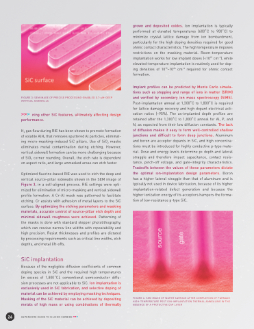
                                  FIGURE 3: SEM IMAGE OF PRECISE PROCESSING-ENABLED 0.7-μM–DEEP VERTICAL SIDEWALLS
ning other SiC features, ultimately affecting design performance.
H2 gas flow during RIE has been shown to promote formation of volatile AlH3 that removes sputtered Al particles, eliminat- ing micro-masking–induced SiC pillars. Use of SiO2 masks eliminates metal contamination during etching. However, vertical sidewall formation can be more challenging because of SiO2 corner rounding. Overall, the etch rate is dependent on aspect ratio, and large unmasked areas can etch faster.
Optimized fluorine-based RIE was used to etch the deep and vertical source-pillar sidewalls shown in the SEM image of Figure 3, in a self-aligned process. RIE settings were opti- mized for elimination of micro-masking and vertical sidewall profile formation. A Cr-Al mask was patterned to facilitate etching. Cr assists with adhesion of metal layers to the SiC surface. By optimizing the etching parameters and masking materials, accurate control of source-pillar etch depth and minimal sidewall roughness were achieved. Patterning of the masks is done with standard stepper photolithography, which can resolve narrow line widths with repeatability and high precision. Resist thicknesses and profiles are dictated by processing requirements such as critical line widths, etch depths, and metal lift-offs.
SiC implantation
Because of the negligible diffusion coefficients of common doping species in SiC and the required high temperatures (in excess of 1,800˚C), conventional semiconductor diffu- sion processes are not applicable to SiC. Ion implantation is exclusively used in SiC fabrication, and selective doping of material can be achieved by employing masking techniques. Masking of the SiC material can be achieved by depositing metals of high mass or using combinations of thermally
grown and deposited oxides. Ion implantation is typically performed at elevated temperatures (600˚C to 900˚C) to minimize crystal lattice damage from ion bombardment, particularly for the high doping densities required for good ohmic contact characteristics. The high temperature imposes restrictions on the masking material. Room-temperature implantation works for low implant doses (<1015 cm–2), while elevated-temperature implantation is routinely used for dop- ing densities of 1019–1020 cm–3 required for ohmic contact formation.
Implant profiles can be predicted by Monte Carlo simula- tions such as stopping and range of ions in matter (SRIM) and verified by secondary ion mass spectroscopy (SIMS). Post-implantation anneal at 1,300˚C to 1,800˚C is required for lattice damage recovery and high dopant electrical acti- vation ratios (~95%). The as-implanted depth profiles are retained after the 1,300˚C to 1,800˚C anneal for Al, P, and N, as expected from their low diffusion constants. The lack of diffusion makes it easy to form well-controlled shallow junctions and difficult to form deep junctions. Aluminum and boron are acceptor dopants in SiC, and high concentra- tions must be introduced for highly conductive p-type mate- rial. Dose and energy levels determine p+ depth and lateral straggle and therefore impact capacitance, contact resis- tance, pinch-off voltage, and gate-integrity characteristics. Tradeoffs between the values of these parameters dictate the optimal ion-implantation design parameters. Boron has a higher lateral straggle than that of aluminum and is typically not used in device fabrication, because of its higher implantation-related defect generation and because the higher ionization energy of its acceptors hampers the forma- tion of low-resistance p-type SiC.
FIGURE 4: SEM IMAGE OF WAFER SURFACE AFTER COMPLETION OF FURNACE HIGH-TEMPERATURE POST ION-IMPLANTATION THERMAL ANNEALING IN THE ABSENCE OF A PROTECTIVE CAP LAYER
     26
ASPENCORE GUIDE TO SILICON CARBIDE
