Page 24 - mlcc-170613
P. 24
MULTILAYER CERAMIC CAPACITORS

          9.3  印刷電路板設計  (PCB design)


           9.3.1 印刷電路板設計(PCB design)

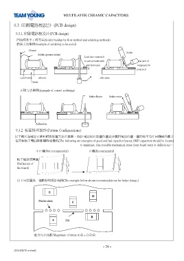
            回流焊及手工焊方法(Solder buildup by flow method and soldering methods)
            錯誤方法舉例(Example of soldering to be avoid)

                    Chassis
                                                                                                                                                                                                Solder
                          Solder (ground solder)
                                                                                                                            Lead wire connected
                                                                                                                            to part provided with                                                      lead wire of
                                                                                                                              with lead wires                                                            component be
                                                                                                                                                                                                                connected

              Land Pattern          adhesive                                                                                      other parts
                                Copper

              正確方法舉例(Example of correct soldering)

                                                           Solder Resist     Solder resist


                                  Adhesive

           9.3.2  板面排列設計(Pattern Configurations)
           以下圖片為電容正確和錯誤放置方法示意圖,SMD 電容貼片放置位置設計應將電容位置,置於較不受任何機械外應力
           位置使板子彎曲降影響降到最低(The following are examples of good and bad capacitor layout; SMD capacitors should be located
                                                     to minimize. Any possible mechanical stress from board warp or deflection.)。
                                      不正確(Not recommended)                          正確(Recommended)

            板子偏斜或彎曲
            (Reflection of
            the board)


            以下示意圖為一個較好的設計範例(The example below shows recommendations for better design.)


                                 E
                                                             D
                          Perforation           C


                                                            B
                                   A       Slit


                                    應力大小比較 Magnitude of stress A>B = C>D>E


                                                                                                          - 24 -
          (2016/08/10 revised)

