


Page 1078 - Basic Electrical Engineering
P. 1078
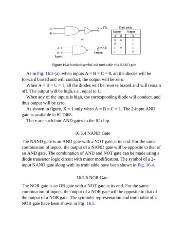
Figure 16.4 Standard symbol and truth table of a NAND gate


                  As in Fig. 16.3 (a), when inputs A = B = C = 0, all the diodes will be
               forward biased and will conduct, the output will be zero.

                  When A = B = C = 1, all the diodes will be reverse biased and will remain
               off. The output will be high, i.e., equal to 1.

                  When any of the inputs is high, the corresponding diode will conduct, and
               thus output will be zero.
                  As shown in figure, X = 1 only when A = B = C = 1. The 2-input AND

               gate is available in IC 7408.
                  There are such four AND gates in the IC chip.


                                                   16.5.4 NAND Gate


               The NAND gate is an AND gate with a NOT gate at its end. For the same
               combination of inputs, the output of a NAND gate will be opposite to that of

               an AND gate. The combination of AND and NOT gate can be made using a
               diode transistor logic circuit with minor modification. The symbol of a 2-

               input NAND gate along with its truth table have been shown in Fig. 16.4.


                                                    16.5.5 NOR Gate

               The NOR gate is an OR gate with a NOT gate at its end. For the same

               combination of inputs, the output of a NOR gate will be opposite to that of
               the output of a NOR gate. The symbolic representation and truth table of a

               NOR gate have been shown in Fig. 16.5.

