


Page 997 - Basic Electrical Engineering
P. 997
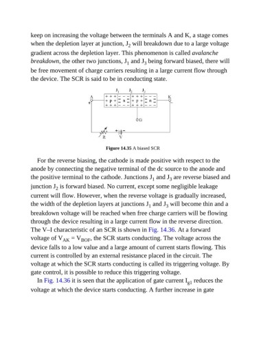
keep on increasing the voltage between the terminals A and K, a stage comes
               when the depletion layer at junction, J  will breakdown due to a large voltage
                                                             2
               gradient across the depletion layer. This phenomenon is called avalanche
               breakdown, the other two junctions, J  and J  being forward biased, there will
                                                            1
                                                                     3
               be free movement of charge carriers resulting in a large current flow through
               the device. The SCR is said to be in conducting state.


                                                   Figure 14.35 A biased SCR

                  For the reverse biasing, the cathode is made positive with respect to the

               anode by connecting the negative terminal of the dc source to the anode and
               the positive terminal to the cathode. Junctions J  and J  are reverse biased and
                                                                                3
                                                                        1
               junction J  is forward biased. No current, except some negligible leakage
                           2
               current will flow. However, when the reverse voltage is gradually increased,
               the width of the depletion layers at junctions J  and J  will become thin and a
                                                                               3
                                                                       1
               breakdown voltage will be reached when free charge carriers will be flowing
               through the device resulting in a large current flow in the reverse direction.

               The V–I characteristic of an SCR is shown in Fig. 14.36. At a forward
               voltage of V   AK   = V BOF , the SCR starts conducting. The voltage across the

               device falls to a low value and a large amount of current starts flowing. This
               current is controlled by an external resistance placed in the circuit. The

               voltage at which the SCR starts conducting is called its triggering voltage. By
               gate control, it is possible to reduce this triggering voltage.

                  In Fig. 14.36 it is seen that the application of gate current I  reduces the
                                                                                         g1
               voltage at which the device starts conducting. A further increase in gate

