


Page 993 - Basic Electrical Engineering
P. 993
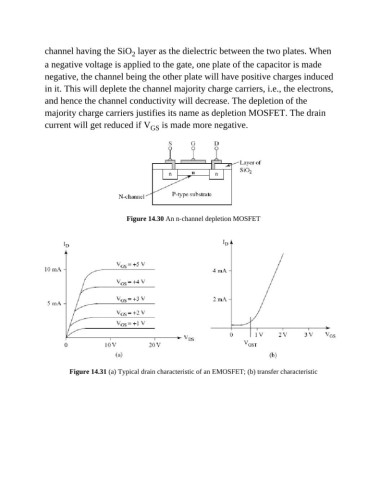
channel having the SiO  layer as the dielectric between the two plates. When
                                           2
               a negative voltage is applied to the gate, one plate of the capacitor is made

               negative, the channel being the other plate will have positive charges induced
               in it. This will deplete the channel majority charge carriers, i.e., the electrons,

               and hence the channel conductivity will decrease. The depletion of the
               majority charge carriers justifies its name as depletion MOSFET. The drain
               current will get reduced if V  is made more negative.
                                                 GS


                                          Figure 14.30 An n-channel depletion MOSFET


                       Figure 14.31 (a) Typical drain characteristic of an EMOSFET; (b) transfer characteristic

