


Page 988 - Basic Electrical Engineering
P. 988
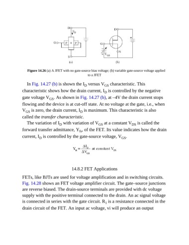
Figure 14.26 (a) A JFET with no gate-source bias voltage; (b) variable gate-source voltage applied
                                                          to a JFET

                  In Fig. 14.27 (b) is shown the I  versus V  characteristic. This
                                                                     GS
                                                        D
               characteristic shows how the drain current, I  is controlled by the negative
                                                                     D
               gate voltage V . As shown in Fig. 14.27 (b), at –4V the drain current stops
                                 GS
               flowing and the device is at cut-off state. At no voltage at the gate, i.e., when

               V  is zero, the drain current, I  is maximum. This characteristic is also
                  GS
                                                     D
               called the transfer characteristic.
                  The variation of I  with variation of V  at a constant V  is called the
                                       D
                                                                 GS
                                                                                      DS
               forward transfer admittance, Y , of the FET. Its value indicates how the drain
                                                    fs
               current, I  is controlled by the gate-source voltage, V .
                          D
                                                                                GS


                                               14.8.2 FET Applications

               FETs, like BJTs are used for voltage amplification and in switching circuits.
               Fig. 14.28 shows an FET voltage amplifier circuit. The gate–source junctions

               are reverse biased. The drain-source terminals are provided with dc voltage
               supply with the positive terminal connected to the drain. An ac signal voltage

               is connected in series with the gate circuit. R  is a resistance connected in the
                                                                     1
               drain circuit of the FET. An input ac voltage, vi will produce an output

