


Page 987 - Basic Electrical Engineering
P. 987
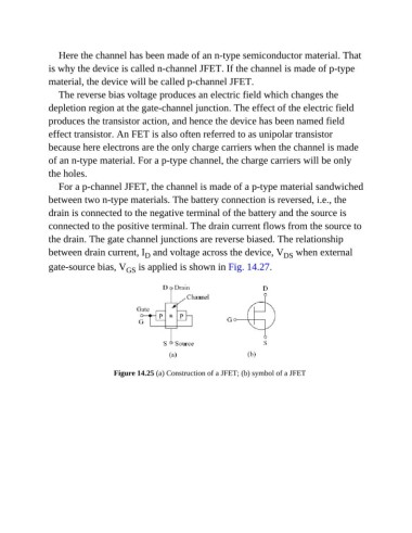
Here the channel has been made of an n-type semiconductor material. That
               is why the device is called n-channel JFET. If the channel is made of p-type
               material, the device will be called p-channel JFET.

                  The reverse bias voltage produces an electric field which changes the
               depletion region at the gate-channel junction. The effect of the electric field

               produces the transistor action, and hence the device has been named field
               effect transistor. An FET is also often referred to as unipolar transistor

               because here electrons are the only charge carriers when the channel is made
               of an n-type material. For a p-type channel, the charge carriers will be only

               the holes.
                  For a p-channel JFET, the channel is made of a p-type material sandwiched
               between two n-type materials. The battery connection is reversed, i.e., the

               drain is connected to the negative terminal of the battery and the source is
               connected to the positive terminal. The drain current flows from the source to

               the drain. The gate channel junctions are reverse biased. The relationship
               between drain current, I  and voltage across the device, V  when external
                                                                                     DS
                                            D
               gate-source bias, V  is applied is shown in Fig. 14.27.
                                      GS


                                   Figure 14.25 (a) Construction of a JFET; (b) symbol of a JFET

