


Page 989 - Basic Electrical Engineering
P. 989
voltage change across the device, i.e., VD. The ratio of the output voltage to
               the input voltage is called voltage amplification of the circuit, A .
                                                                                            v


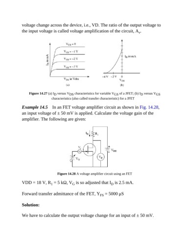
                    Figure 14.27 (a) I  versus V DS  characteristics for variable V GS  of a JFET; (b) I  versus V GS
                                     D
                                                                                              D
                                   characteristics (also called transfer characteristic) for a JFET
               Example 14.5    In an FET voltage amplifier circuit as shown in Fig. 14.28,

               an input voltage of ± 50 mV is applied. Calculate the voltage gain of the
               amplifier. The following are given:


                                       Figure 14.28 A voltage amplifier circuit using an FET

               VDD = 18 V, R  = 5 kΩ, V  is so adjusted that I  is 2.5 mA.
                                                 G
                                                                          D
                                   1
               Forward transfer admittance of the FET, Y  = 5000 μS
                                                                   FS


               Solution:


               We have to calculate the output voltage change for an input of ± 50 mV.

