
Page 39 - GIGABYTE Service Manual-v3.0-110101
P. 39
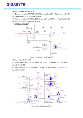
Design 2: Control by SI3443DV

                   01. Before powered on, PWROK1, LM393 pin1, pin7 and SI3443 pin3 are low, Q184 is
                   off, and so 5VDUAL is provided by 5VSB.
                   02. After powered on, PWROK1, LM393 pin1, pin7 and SI3443 pin3 are high, Q184 is
                   on, and so 5VDUAL is provided by VCC.


                                            Figure 2-17: Control by SI3443DV
                   Design 3: Transfer by 9435

                   01. Before powered on, U17 393 output low, Q37 off, Q293 9435 on, 5VDUAL is
                   provided by 5VSB.
                   02. After powered on, U17 393 output high, Q37 on, Q293 9435 off, 5VDUAL is

                   provided by VCC.


                                              Figure 2-18: Transfer by 9435

                                                            17