Page 310 - Mechatronics with Experiments
P. 310

JWST499-Cetinkunt
            JWST499-c05
                       296   MECHATRONICS  Printer: Yet to Come                     October 28, 2014 11:15 254mm×178mm
                                                                       V out
                                                                   5 V


                              V in                     V out                         V
                                                                         2 3 4 V      in


                                       (a)                                (b)
                                           V in


                                       V ht

                                       V LT


                                                                                      Time
                                             IC
                                            input


                                                                                      Time
                                    Schmitt  IC
                                    trigger  input
                                    output


                                                                                      Time
                                                               (c)
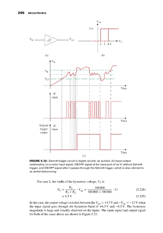
                              FIGURE 5.32: Schmitt trigger circuit in digital circuits: (a) symbol, (b) input–output
                              relationship, (c) a noisy input signal, ON/OFF signal at the input port of an IC without Schmitt
                              trigger, and ON/OFF signal after it passes through the Schmitt trigger, which is also referred to
                              as switch-debouncing.


                                   For case 2, the width of the hysteresis voltage, V is
                                                                         T
                                                      R 2             100 000
                                               V =         ⋅ V sat  =            ⋅ 13           (5.228)
                                                T
                                                    R + R 2       100 000 + 100 000
                                                     1
                                                  = 6.5 V                                       (5.229)
                              In this case, the output voltage switches between the V sat  =+13 V and −V sat  =−13 V when
                              the input signal goes through the hysteresis band of +6.5 V and −6.5 V. The hysteresis
                              magnitude is large and visually observed on the figure. The input signal and output signal
                              for both of the cases above are shown in Figure 5.33.
   305   306   307   308   309   310   311   312   313   314   315