


Page 1112 - Basic Electrical Engineering
P. 1112
A monolithic circuit is a complete circuit having active and passive circuit
               components and their interconnections made on a single chip (the word
               monolithic is derived from a Greek word mono = single, lithic = stone or

               piece). Integrated circuit technology has developed small scale integration to
               very large scale integration. Small scale integration (SSI) has less than 12

               gates on a single chip while very large scale integration (VLSI) has over 1000
               gates in a single chip.


                                         17.2 FABRICATION OF MONOLITHIC ICS

               The fabrication of ICs involves a very special and sophisticated technology.
               Here we will briefly mention only the steps involved. The steps are as

               follows:

                   i.  Wafer preparation: Wafer is a very thin surface of p-type silicon which provides the base or
                     substrate on which the circuit elements are grown or developed. Wafers are made by slicing a
                     p-type round silicon material of certain diameter. These wafers are polished to a mirror finish
                     surface.
                  ii.  Epitaxial growth: On the p-type substrate an n-type layer is grown by placing the wafer in a
                     furnace in an atmosphere of phosphorous gas at 1200°C. Thus, an epitaxial layer of n-type
                     material is formed on the p-type wafer.
                  iii.  Diffused isolation: A thin layer of silicon dioxide is formed on the n-type layer by oxidation
                     method, i.e., by oxidizing the wafer in dry oxygen. Next, a thin coating of a chemical, called
                     photoresist is made on the SiO  layer.
                                                 2


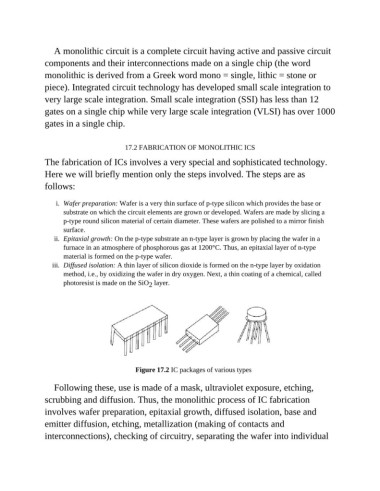
                                             Figure 17.2 IC packages of various types


                  Following these, use is made of a mask, ultraviolet exposure, etching,
               scrubbing and diffusion. Thus, the monolithic process of IC fabrication
               involves wafer preparation, epitaxial growth, diffused isolation, base and

               emitter diffusion, etching, metallization (making of contacts and
               interconnections), checking of circuitry, separating the wafer into individual

