


Page 1116 - Basic Electrical Engineering
P. 1116
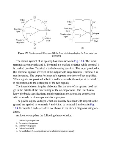
Figure 17.3 Pin diagrams of IC op-amp 741. (a) 8-pin mini dip packaging; (b) 8-pin metal can
                                                          packaging

                  The circuit symbol of an op-amp has been shown in Fig. 17.4. The input

               terminals are marked a and b. Terminal a is marked negative while terminal b
               is marked positive. Terminal a is the inverting terminal. The input provided at

               this terminal appears inverted at the output with amplification. Terminal b is
               non-inverting. The output for input at b appears non-inverted but amplified.

               When signals are provided at both a and b terminals, the output at terminal c
               is proportional to the difference of the two signals.

                  The internal circuit is quite elaborate. But the user of an op-amp need not
               go to the details of the functioning of the op-amp circuit. The user has to
               know the basic specifications and the terminals so as to make connections

               with external circuit components for a purpose.
                  The power supply voltages which are usually balanced with respect to the

               ground are applied to terminals 7 and 4, i.e., to terminal d and e as in Fig.
               17.4 Terminals d and e are often not shown in the circuit diagrams using op-
               amps.

                  An ideal op-amp has the following characteristics:


                   i.  Infinite input impedance
                  ii.  Zero output impedance
                  iii.  Infinite voltage gain
                  iv.  Infinite bandwidth
                   v.  Perfect balance (i.e., output is zero when both the inputs are equal)

